Dos resultados do Q2
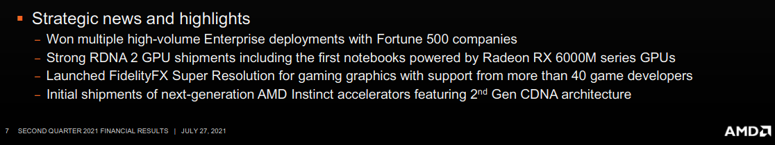
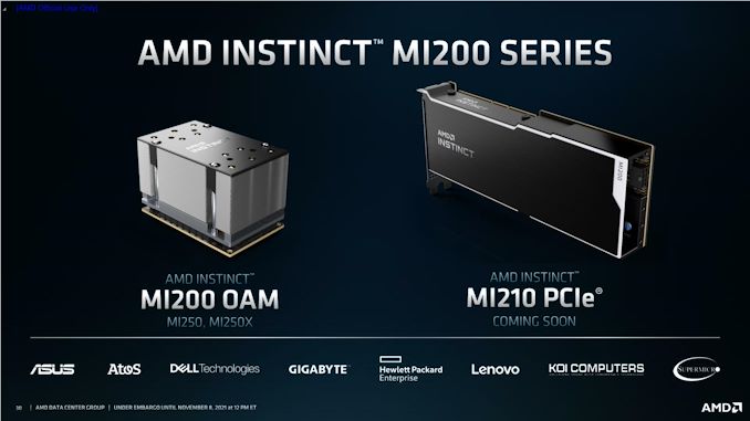
Initial shipments of next-generation AMD Instinct featuring 2nd Gen CDNA
Initial shipments of next-generation AMD Instinct featuring 2nd Gen CDNA

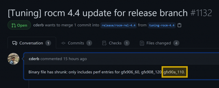
https://videocardz.com/newz/amd-ins...aldebaran-gpu-might-feature-110-compute-unitsThe code lists GFX906_60 which is assumed to be Instinct MI60, GFX908_120 which is Instinct MI100, and GFX90A_110, more than likely being the next-gen flagship accelerator from AMD. The GFX numbers are not important here, but the numbers attached to those GPU architecture IDs are. The 60 stands for 60 Compute Units, a configuration of MI60, while 120 stands for 120 Compute Units for Instinct MI100. The 110 would therefore be a configuration of MI200. Thus, the graphics accelerator would feature 110 Compute Units, 10 fewer than Arcturus. This number is likely referring to a single GPU chiplet, which is why the full solution should offer 220 Compute Units.

")


Podes ter todo o tipo de áreas a usar GPUs. Desde minar cryptocoins, Simulações de CFD por parte de uma equipa de Formula 1, estudo de energia nuclear até coisas menos comuns em GPUs, como Bases de Dados.Que tipo de uso tem uma besta dessas? É para R&D em medicina ou ciência? Usar como AI?


All of these IF links are 16 bits wide an operate at 25Gbps in a dual simplex fashion. This means there’s 50GB/second of bandwidth up and another 50GB/second of bandwidth down along each link. Or, as AMD likes to put it, each IF link is 100GB/second of bi-directional bandwidth, for a total aggregate bandwidth of 800GB/second. Notably, this gives the two GCDs within an MI250(X) 200GB/second of bandwidth in each direction to communication among themselves. This is an immense amount of bandwidth, but for remote memory accesses it’s still going to be a fraction of the 1.6TB/second available to each GCD from its own HBM2E memory pool.
However, besides EMIB being an Intel technology, it’s not without its own drawbacks, so AMD and its fab partners think they can do one better than that. And that one better thing is Elevated Fanout Bridge 2.5D.
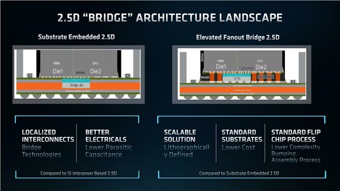
So what makes Elevated Fanout Bridge 2.5D different? In short, EFB builds above the substrate, rather than inside it. In this case, the entire chip pair – the GPU and the HBM stack – are placed on top of a mold with a series of copper pillars in it. The copper pillars allow the coarse-pitched contacts on the chips to make contact with the substrate below in a traditional fashion. Meanwhile, below the high-precision, fine-grained microbumps used for HBM, a silicon bridge is instead placed. The end result is that by raising the HBM and GPU, it creates room to put the small silicon bridge without digging into the substrate.
Compared to a traditional interposer, such as what was used on the MI100, the benefits are obvious: even with the added steps of using EFB, it still avoids having to use a massive and complex silicon interposer.
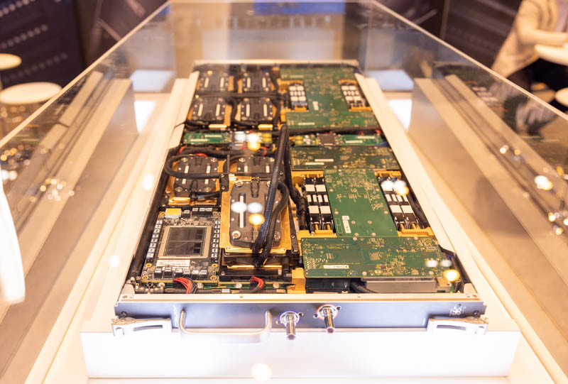
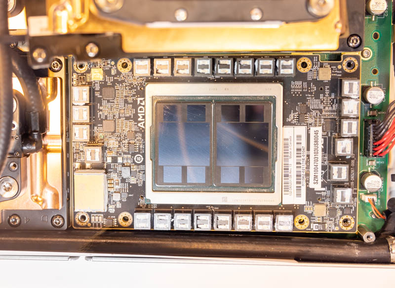
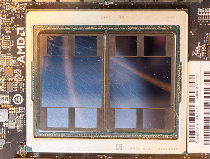
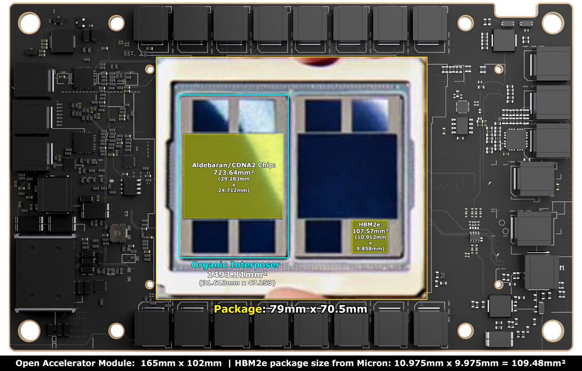
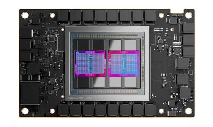
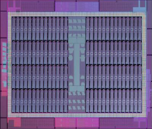
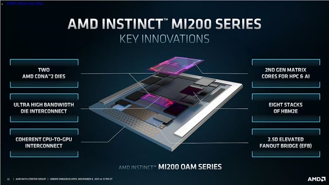
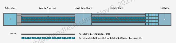
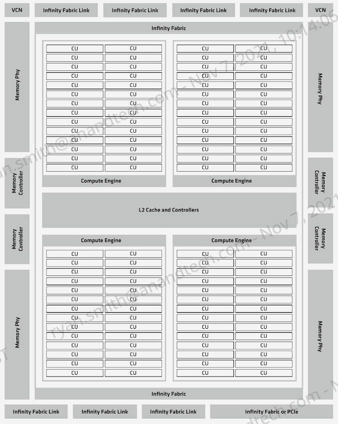
The GCD is a modest chip built on TSMC’s N6 process technology, making this the first AMD product built on that line. According to AMD each GCD is 29 billion transistors, and at least for the moment, AMD isn’t sharing anything about die sizes. As far as major functional blocks go, the GCD contains 112 CUs, which are organized into 4 Compute Engines. This is paired with 4 HBM2E memory controllers, and 8 Infinity Fabric Links.
The upshot of a more modest transistor count and the smaller manufacturing process is that it opens the door to AMD embracing a chiplet-like design approach for their accelerators.
These two GPUs, in turn, are functionally independent of each other; but both are connected to the other via 4 Infinity Fabric links. This sets MI200 apart from previous AMD multi-GPU server offerings, as those products were all connected via the non-coherent PCIe bus.
AMD is using 16GB HBM2E stacks here, which gives each GCD 64GB of memory, or a cumulative total of 128GB for the full package.
However all of this performance and memory comes at a cost: power consumption. To get the best performance out of the MI250(X) you’ll need to liquid cool it to handle its 560W TDP. Otherwise, the highest air-cooled configuration is still some 500W.
Given that AMD is using two GPUs in an accelerator, such a high TDP is not all that surprising. But it does mean that a full, 8-way configuration – which is a supported configuration – will require upwards of 5000W just for the accelerators, never mind the rest of the system.
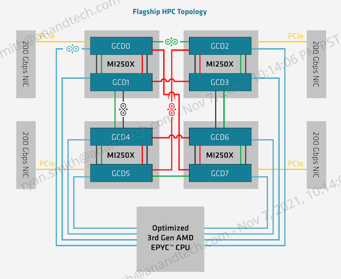
With the additional IF links exposed by the OAM form factor, AMD has given each GCD 8 Infinity Fabric 3.0 links. As previously mentioned, 4 of these links are used to couple the two GCDs within an MI200, which leaves 4 IF links per GCD (8 total) free for linking up to hosts and other accelerators
All of these IF links are 16 bits wide an operate at 25Gbps in a dual simplex fashion. This means there’s 50GB/second of bandwidth up and another 50GB/second of bandwidth down along each link. Or, as AMD likes to put it, each IF link is 100GB/second of bi-directional bandwidth, for a total aggregate bandwidth of 800GB/second. Notably, this gives the two GCDs within an MI250(X) 200GB/second of bandwidth in each direction to communication among themselves. This is an immense amount of bandwidth, but for remote memory accesses it’s still going to be a fraction of the 1.6TB/second available to each GCD from its own HBM2E memory pool.
Otherwise, these links run at the same 25Gbps speed when going off-chip to other MI250s or an IF-equipped EPYC CPU. Besides the big benefit of coherency support when using IF, this is also 58% more bandwidth than what PCIe 4.0 would otherwise be capable of offering.
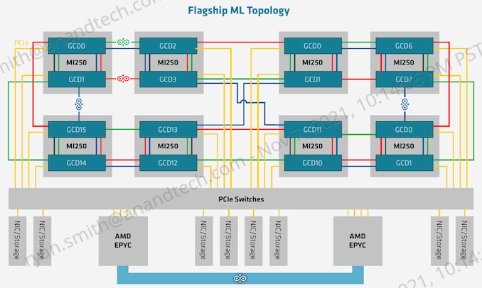
The 8 free IF links per package means that the MI250(X) can be installed into a number of different topologies. AMD’s favored topology, which is being used Frontier’s nodes, is a 4+1 setup with 4 accelerators attached to a single EPYC CPU via IF links, for a fully coherent setup. In this case each GCD has its own IF link to the CPU, and then there are 3 more links available to each GCD to connect with other GCDs. The net result is that it’s not a fully-connected setup – some GCDs will have to go through another GCD to reach any given GPU – but it accomplishes full coherency across all of the GPUs and with the CPU.
And while IF is clearly the most preferred method of communication, for customers who either can’t get or don’t need the special Epyc CPUs required, the master IF link in each GCD can also be used for PCIe communication. In which case the topology is the same, but each GPU is linked back to its host CPU by PCIe instead. And for the very adventurous ML server operators, it’s also possible to build an 8-way MI250(X) topology, which would result in 16 CDNA 2 GCDs inside a single system.
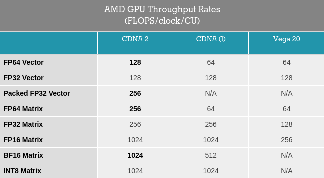
What AMD’s diagrams don’t show is that the width of each ALU/shader core within a CU has been doubled. CDNA 2’s ALUs are 64-bit throughout, allowing the architecture to process FP64 operations at full speed. This is twice the rate of MI100, where FP64 operations ran at one-half the rate of FP32 operations.
All of this underscores the different directions AMD and NVIDIA have gone; for Ampere, NVIDIA invested almost everything in matrix performance, to the detriment of significantly improving vector performance. AMD on the other hand has gone the other direction; overall throughput per matrix core hasn’t really improved, but vector SIMD performance has.
Meanwhile, AMD has also given their Matrix Cores a very similar face-lift. First introduced in CDNA (1), the Matrix Cores are responsible for AMD’s matrix processing. And for CDNA 2, they’ve been expanded to allow full-speed FP64 matrix operations as well, bringing them up to the same 256 FLOPS rate as FP32 matrix operations, a 4x improvement over the old 64 FLOPS/clock/CU rate. Unlike the vector ALUs, however, there are no packed operations or other special cases to take advantage of, so this change doesn’t improve FP32/FP16 performance, which remains at 256 FLOPS and 1024 FLOPS per clock respectively.
Finally, while CDNA 2 is primarily compute-focused, not every last transistor is dedicated to the task. Like its predecessor, CDNA 2 also includes a new version of AMD’s Video Codec Next (VCN) block, which is responsible for video encode and decode acceleration. Judging from AMD’s comments on the matter, this would seem to be included more for decode acceleration than any kind of video encoding tasks, as fast decode capabilities are needed to disassemble photos and videos for use in ML training. This version of the VCN does not support AV1, so the highest format supported for encode/decode is HEVC.
AMD began the first shipments of MI250X parts for the Frontier supercomputer back in Q3 of this year, and they are continuing to ship them in order to fill the US Department of Energy’s order for tens-of-thousands of GPUs.
In the meantime, AMD won’t be alone in their journey. After the Frontier order is complete, AMD will be able to begin focusing on ODM and OEM orders, with ODM/OEM availability expected in the first quarter of next year.

Bom além do Frontier ainda têm o Lumi e o Pawsey, se entretanto não ganharem mais nenhum.
Adastra – a partial conjoining of the famous phrase “ad astra per aspera” (Latin for “to the stars through hardship”) – will consist of two complementary partitions.
The first partition, scheduled to be operational by spring 2022, will consist of manycore scalar nodes based on next-gen AMD Epyc Genoa CPUs and 700GB of DDR5 memory per node, all networked with HPE Slingshot 11 (200Gbps).
https://www.hpcwire.com/2021/11/15/hpe-amd-to-power-new-french-supercomputer-adastra/The second partition’s nodes, slated for operation by Q4 2022, will complement a third-gen AMD Epyc CPU with 256GB of DDR4 memory and quadruple AMD Instinct MI250X OAM GPUs, again networked by HPE Slingshot 11 (200Gbps).