
The Golden Eagle
I quit My Job for Folding
Essas boards de dois sockets são coisas para custar >500€?
E já agora, quanto deve custar um Opteron de 6cores?
Cumps
E já agora, quanto deve custar um Opteron de 6cores?
Cumps
Essas boards de dois sockets são coisas para custar >500€?
Vai sair várias boards EATX (12"x13" (305x330mm)) que muitas caixas para desktop suportam.
Para um PC normal, para jogos pouco ganham com boards para servidores/workstations...
ha algum impedimento em usar DDR3 normal?
Multiple DDR3 DIMM types are supported:
Registered DIMMs (RDIMM)
ECC unbuffered DIMMs (UDIMM ECC)
Unbuffered DIMMs (UDIMM)
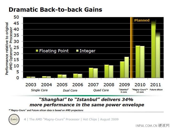
Enter Interlagos and Valencia; AMD's first processors based on the revolutionary [for AMD, of course] CPU architecture. According to released information, a 170% increase in number of cores [from 6 to 16] should result in 400% performance increase in Floating-Point calculations on a clock-per-clock basis. Add variant clocks to that and we have a receipt for a hard battle in server/workstation segment. Valencia's theoretical numbers should show similar jumps, but overall performance will differ due to difference in memory controller: Valencia comes with a dual-channel, 144-bit memory controller while Interlagos features a quad-channel, 288-bit memory controller.
According to the call, it can be expected that Bulldozer will be a seriously big deal for the CPU space. While Bobcat targets the low-end and wants to go after spreading ARM and its Cortex series, Bulldozer is the first new CPU architecture for AMD since Hammer series in 2003. While Patla wasn't willing to disclose interesting architectural details that would explain the impressive jump in projected performance for the Bulldozer-based Interlagos processor.
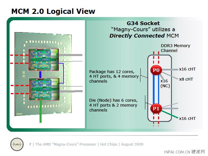
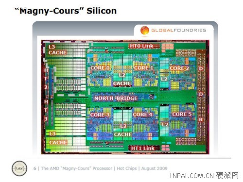
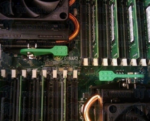
Magny-Cours MCM and links
Here is where the fun begins, with the MCM itself. The red links are memory channels, two per die, four per socket. Green, blue and grey are all HT, with wide lines representing 16-bit links, narrow ones are 8-bit. It doesn't take much to realize that things are complex here.
The wide green link off the bottom is is the external I/O, basically the connection to the chipset, one per socket. Actually, since you can "ungang" the 16-bit HT link into two 8-bit HT links, you could theoretically put two chipsets off of one socket. That said, this is very unlikely to happen, it is much easier to add one off each socket.
This link is non-coherent HT (ncHT), meaning that it can't be used for CPU to CPU interconnects. All of the other links, blue and grey are cache-coherent HT (ccHT). If you are sharp eyed, you will notice that the blue ccHT links between the dies on package are different widths.
The 'extra' link is extra for a good reason, but more on this later. AMD added it to the mix because it could, more or less for free. It increased the bandwidth between the cores by 50%, but real world performance does not go up by much because the cores are rarely bandwidth bound.
Of more interest is that, because these dies are soldered to the package, not run through a socket, they are of a set length and made of known materials. AMD took some liberties here, basically because it can keep tolerances much tigher; it upped the bandwidth on these links a lot. Unfortunately, AMD did not say how much. The links are ccHT like all the other, just notably faster and likely lower latency as well.
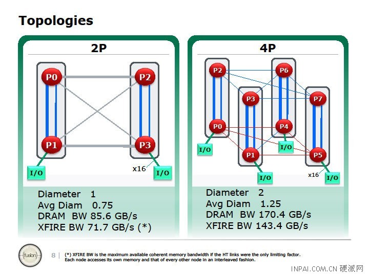
In a four socket system using the 'old way' AMD did things, that is, a square, two of these three links were used to connect the chips to the two neighbors. A chip in the top left would be connected to the one on the right, and the one below, but not the socket diagonally across. The third was not used.
Diagonal connections could be done, but rarely if ever actually were done. The third ccHT connection was used to connect two 4-way squares to make an 8-way system. While this was a good thing for packing more CPUs into a box, it was hobbled by the latency caused by multiple hops across HT links. CPU 0 loading from CPU 7's memory might need four hops to get to the data and four hops to get back. Add in cache coherency, and you had those hops taking the whole system to its knees.
The way around this is to directly connect each socket to every other one in the system. On a two socket box, that is easy, you just connect point A to point B. On a four socket, you make a square with an X in the middle, exactly what AMD traded off to allow for eight sockets on socket F and before.
With the new socket G34, AMD did just that. The grey 8-bit ccHT link is basically a diagonal link, the X in the square. If there was only one die in each socket, that would work wonderfully, problem solved! Unfortunately, G34 has two dies per socket, and they are connected to the two dies in the other socket using one of those 8-bit links per die.
On a two socket system, the links directly between the dies are 16-bit and the ones going diagonally are 8-bit. Since there are two full ccHT links per die, there are four per socket to connect everything on a four socket system. To connect between sockets, you don't need the full bandwidth that a 16-bit HT links brings.
In the end, each socket is connected to every other socket directly, but every die is only connected to every other die on a two socket system. The worst case in G34 is to have any die two hops away from any other die. It all looks like this.


Este era daqueles que se tivesse € comprava logo
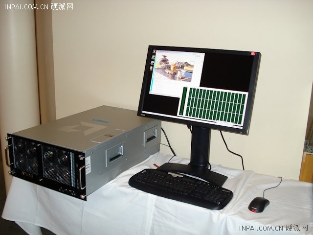
Quem monstro de CPU...quero ver benchs disso
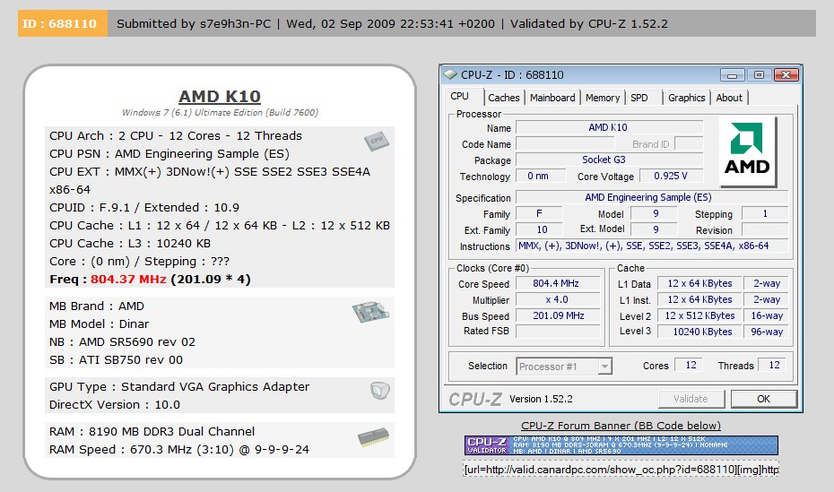
Não sei se repararam, mas naquela plataforma estão dois CPUs com 12 núcleos cada um. Ou seja, 32 núcleos.
É mesmo caso para dizer Holly Shit.
hmmmm acho que são 2 CPUS de 6 cores cada um... ou seja o mesmo que a intel vez para os core 2 que era 2 processadores de um nucleo cada um...
Mas mesmo que seja 2 CPUS de 12 cores cada um:
12
+12
_____
24
ehehehe
 3,5s
3,5s 
