
You are using an out of date browser. It may not display this or other websites correctly.
You should upgrade or use an alternative browser.
You should upgrade or use an alternative browser.
Cell Architecture Explained: Introduction
- Autor do tópico Xpirit
- Data Início
Xpirit
Banido
Nemesis11 disse:Mais on topic:
Como é que ele vai ser barato com um die size de 206mm^2 ?
Aqui dão como 221 mm^2 e 234 milhoes transistores.
Nemesis,
o CELL a usar na PS3 vai ser de 65nm. Neste caso o DIE terá 115mm² (e não estou a contar com circuitos que podem vir a ser cortados nos CELL da PS3) o que já é aceitavel e numa economia de escala atira-o para menos de $100. Os de 90nm são protótipos e mais tarde CELL's para desenvolvimento de software e quem sabe workstations e mais qq coisa.
")
Nemesis11
Power Member
Sim, em 0.065, se não alterarem nada, deve ficar bem mais barato de fabricar.
Mesmo assim não espero que a PS3 tenha mais que 1 Cell.
Imagens do Cell:

Uma SPE:

http://www.electronicsweekly.co.uk/...iChannelID=114&liFlavourID=1&sSearch=&nPage=1
http://www.extremetech.com/article2/0,1558,1761407,00.asp
Mesmo assim não espero que a PS3 tenha mais que 1 Cell.
Imagens do Cell:
Uma SPE:
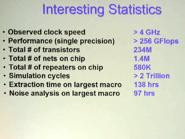
The multi-core processor claims supercomputer-like levels of performance with clock speeds in excess of 4GHz.
A first prototype of the device expected to power the Playstation 3 has a 221mm² die, uses 234 million transistors and is made using 90nm process technology.
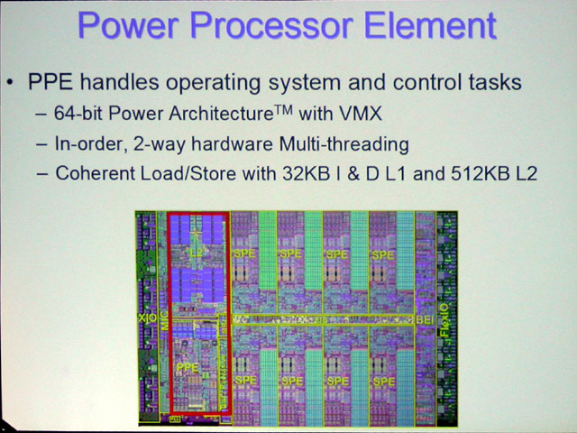
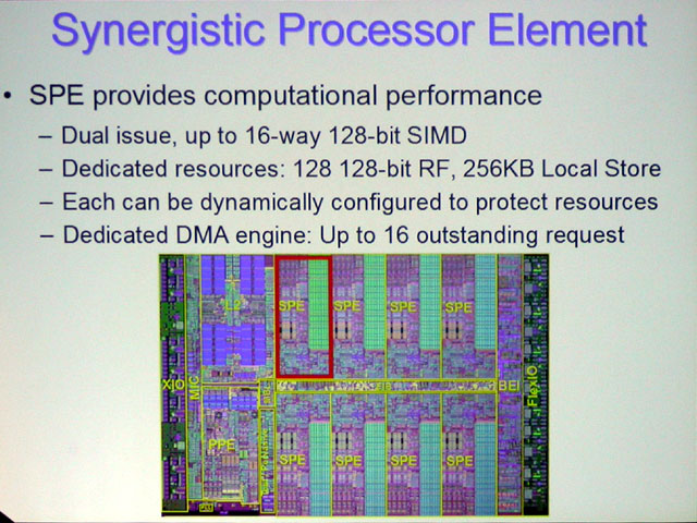
The version of Cell announced today contains eight 64-bit floating point processors, referred to as synergistic processor elements (SPEs). Along side these is a 64-bit Power processor capable of running two threads.
SPEs take 128-bit operands, split into four 32-bit words. Up to 128 operands can be stored in the register file.
Each 2.5x5.81mm SPE can issue two instructions per cycle to seven execution units using two pipelines. There is no out of order execution.
Connecting up the processing units is the element interconnect bus (EIB), comprising four 128-bit rings and a 64-bit tag running at half the processor clock.
The busses connect to the SPEs through local memory, 256kbyte for each SPE. The developers have tested the memories to 5.4GHz at 1.3V and 52°C.
There are 15 separate power domains on the chip. Ten digital thermometers monitor the chip at various points to alert the system of thermal problems.
http://www.electronicsweekly.co.uk/...iChannelID=114&liFlavourID=1&sSearch=&nPage=1
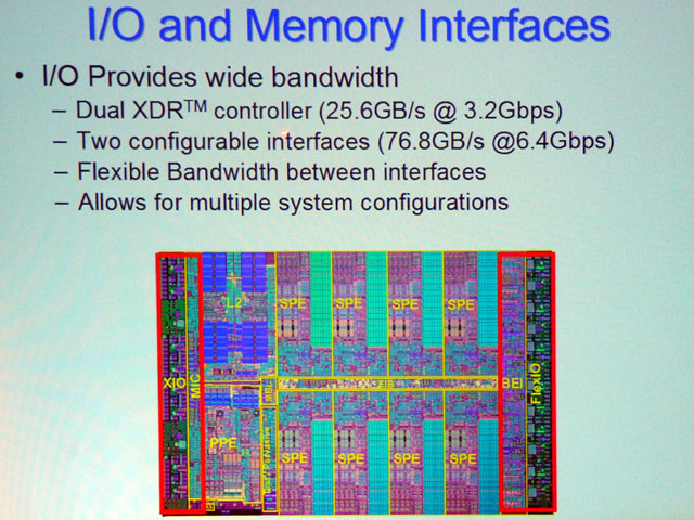
The Cell processor uses two technologies from Rambus: a chip-to-chip interconnect, FlexIO, formerly known as "Redwood"; and an eXtended Data RAM (XDR) interface. Sony indicated in January 2003 that it would use the FlexIO and XDR technology in future game consoles in conjunction with the Cell microprocessor.
The FlexIO technology will be used to connect the various chips on a Cell-based motherboard, according to Rich Warmke, marketing director of the memory interface division at Rambus. A multicore Cell processor, by contrast, will use its own internal bus to connect multiple cores. However, 90 percent of the Cell's external pins are connected to either the FlexIO or XDR interfaces, evidence that the Cell's design emphasizes moving application and or 3D scene data around within main memory, Warmke said.
In total, the two interfaces combined can offer up to 100 Gbytes per second of total bandwidth, an order of magnitude above some other devices, Warmke said.
The FlexIO interface runs at 6.4-GHz, while the XDR interface runs at half of that speed, or 3.2-GHz. Warmke declined to offer specifics on the bandwidth mismatch. "We worked with Sony to understand their needs," he said. "With that application, that ratio of bandwidth was appropriate. Other applications may require more memory bandwidth and less chip-to-chip bandwidth."
http://www.extremetech.com/article2/0,1558,1761407,00.asp
Última edição:
Xpirit
Banido
Each 2.5x5.81mm SPE can issue two instructions per cycle to seven execution units using two pipelines. There is no out of order execution.
"There is no out of order execution."
Será que é por isto que o Hannibal acha que a Apple não vai usar CELL's no futuro? Compreendo o seu raciocínio. Um Power com 8 SPE's que não vão ser muito úteis para correr programas comuns pode vir a ser uma coisa cara para o que é ou um canhão para matar uma mosca. Se é por isto está errado.
Xpirit
Banido
"Each SPU has 256KB local SRAM which is not part of system address space (referred to as "untranslated, unguarded and non-coherent"). There is a DMA unit per SPU to manage background transfers to/from system memory space (with MMU). There can be up to 16 pending DMA requests, each of up to 16kb."
Bolas, quem serão os gajos que estão a fazer os primeiros jogos da PS3? Ainda bem que não tenho nada a haver com o assunto.
Bolas, quem serão os gajos que estão a fazer os primeiros jogos da PS3? Ainda bem que não tenho nada a haver com o assunto.
Nemesis11
Power Member
Uma coisa que reparei é que eles já estão a pensar em Multicores do Cell (que por si já é Multicore)
O PPE tem 512 KB de L2
E a reacção da Intel
http://news.com.com/PlayStation+3+chip+has+split+personality/2100-1043_3-5566340.html
Parece que a Intel não gosta da filosofia do Cell.....
The FlexIO technology will be used to connect the various chips on a Cell-based motherboard, according to Rich Warmke, marketing director of the memory interface division at Rambus. A multicore Cell processor, by contrast, will use its own internal bus to connect multiple cores.
O PPE tem 512 KB de L2
2.5MB of on Chip memory (512KB L2 and 8 * 256KB)
E a reacção da Intel
Some competitors, however, are skeptical that Cell will find much of a home outside of video games. One of the big problems with Cell, said Justin Rattner, an Intel Fellow, is that the processing units aren't identical, a situation that increases complexity and the opportunity for bugs.
"You've got this asymmetry," Rattner said. "It's like having two kinds of motors under the hood. We are very reluctant to adopt architectures like this because they take compatibility and throw it out the window."
http://news.com.com/PlayStation+3+chip+has+split+personality/2100-1043_3-5566340.html
Parece que a Intel não gosta da filosofia do Cell.....
 :rolleyes:")
Xpirit
Banido
ptzs disse:A presentação já deve ter acabado. Quando tiverem mais info avisem, tou acordado.
Acabaram de fazer uma demonstração. Correram o SuperPi em menos de 1s e o 3dmark falhou porque o cálculo do resultado deu out of range.
Amanhã já haverá scans dos papers e possívelmente os slides das apresentações. Novidades destas não acontecem todos os dias. A grande questão a seguir é: Bom, e o que fazer com isto? É a parte mais chata.
|Oc|CRASH_OVer
Suspenso
estas a brincar? nao?
DJ_PAPA
Power Member
Xpirit disse:Acabaram de fazer uma demonstração. Correram o SuperPi em menos de 1s e o 3dmark falhou porque o cálculo do resultado deu out of range.
Amanhã já haverá scans dos papers e possívelmente os slides das apresentações. Novidades destas não acontecem todos os dias. A grande questão a seguir é: Bom, e o que fazer com isto? É a parte mais chata.
Nao acredito! So vendo.............
Aliás, o Superpi tem muitos testes (16kb; 1mb;32 mb; etc) tb dava jeito saber qual deles foi feito. E o Superpi tb so apresenta numeros inteiros. Ou 0 ou 1!
Out of range!!!!! Mas qual dos 3dmarks foi?
Mas eles puseram mesmo o benche a correr e o people viu os testes a decorrer nos 1000 frames ou espetaram so a cena do out of range pro people ver?
A ver vamos como dizia o cego.......... Tou curioso para ver a apresentaçao que eles fizeram........
Axo que por agora é melhor tar um bocado de pé atrás, pq ja se sabe como é o marketing maravilha! Inda por cima de uma nova tecnologia em ascensao!
Eles gostam muito inventar/impressionar o publico.....
Veremos...... com o tempo..........
Última edição:
|Oc|CRASH_OVer
Suspenso
olha se acertavas.... lol
Nemesis11
Power Member
Cá vão os Slides, mas antes que tudo, o Cpu (o package completo e não só o core)
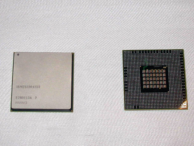
Ena.....Parece um PIV
Agora mais a sério, os slides:
Slides completos:
http://pc.watch.impress.co.jp/docs/2005/0208/kaigaip001.jpg
http://pc.watch.impress.co.jp/docs/2005/0208/kaigaip002.jpg
http://pc.watch.impress.co.jp/docs/2005/0208/kaigaip006.jpg
http://pc.watch.impress.co.jp/docs/2005/0208/kaigaip011.jpg
http://pc.watch.impress.co.jp/docs/2005/0208/kaigaip012.jpg
http://pc.watch.impress.co.jp/docs/2005/0208/kaigaip016.jpg
http://pc.watch.impress.co.jp/docs/2005/0208/kaigaip022.jpg
http://pc.watch.impress.co.jp/docs/2005/0208/kaigaip026.jpg
http://pc.watch.impress.co.jp/docs/2005/0208/kaigaip028.jpg
http://pc.watch.impress.co.jp/docs/2005/0208/kaigaip039.jpg
http://pc.watch.impress.co.jp/docs/2005/0208/kaigaip046.jpg
http://pc.watch.impress.co.jp/docs/2005/0208/kaigaip051.jpg
http://pc.watch.impress.co.jp/docs/2005/0208/kaigaip052.jpg
http://pc.watch.impress.co.jp/docs/2005/0208/kaigaip055.jpg
http://pc.watch.impress.co.jp/docs/2005/0208/kaigaip058.jpg
Outras pics do Cell na ISSCC:
http://pc.watch.impress.co.jp/docs/2005/0208/kaigai002.jpg
http://pc.watch.impress.co.jp/docs/2005/0208/kaigai001.jpg
http://pc.watch.impress.co.jp/docs/2005/0208/kaigai005.jpg
http://pc.watch.impress.co.jp/docs/2005/0208/kaigai008.jpg
http://pc.watch.impress.co.jp/docs/2005/0208/kaigaip053.jpg
Um esquema do Cell:
http://pc.watch.impress.co.jp/docs/2005/0208/kaigai01l.gif
EDIT: A 1ª parte do artigo da Ars
http://arstechnica.com/articles/paedia/cpu/cell-1.ars
Ena.....Parece um PIV
Agora mais a sério, os slides:
Slides completos:
http://pc.watch.impress.co.jp/docs/2005/0208/kaigaip001.jpg
http://pc.watch.impress.co.jp/docs/2005/0208/kaigaip002.jpg
http://pc.watch.impress.co.jp/docs/2005/0208/kaigaip006.jpg
http://pc.watch.impress.co.jp/docs/2005/0208/kaigaip011.jpg
http://pc.watch.impress.co.jp/docs/2005/0208/kaigaip012.jpg
http://pc.watch.impress.co.jp/docs/2005/0208/kaigaip016.jpg
http://pc.watch.impress.co.jp/docs/2005/0208/kaigaip022.jpg
http://pc.watch.impress.co.jp/docs/2005/0208/kaigaip026.jpg
http://pc.watch.impress.co.jp/docs/2005/0208/kaigaip028.jpg
http://pc.watch.impress.co.jp/docs/2005/0208/kaigaip039.jpg
http://pc.watch.impress.co.jp/docs/2005/0208/kaigaip046.jpg
http://pc.watch.impress.co.jp/docs/2005/0208/kaigaip051.jpg
http://pc.watch.impress.co.jp/docs/2005/0208/kaigaip052.jpg
http://pc.watch.impress.co.jp/docs/2005/0208/kaigaip055.jpg
http://pc.watch.impress.co.jp/docs/2005/0208/kaigaip058.jpg
Outras pics do Cell na ISSCC:
http://pc.watch.impress.co.jp/docs/2005/0208/kaigai002.jpg
http://pc.watch.impress.co.jp/docs/2005/0208/kaigai001.jpg
http://pc.watch.impress.co.jp/docs/2005/0208/kaigai005.jpg
http://pc.watch.impress.co.jp/docs/2005/0208/kaigai008.jpg
http://pc.watch.impress.co.jp/docs/2005/0208/kaigaip053.jpg
Um esquema do Cell:
http://pc.watch.impress.co.jp/docs/2005/0208/kaigai01l.gif
EDIT: A 1ª parte do artigo da Ars
L1 cache has been replaced by 256K of locally addressable memory. The SPE's ISA, which is not VMX/Altivec-derivative (more on this below), includes instructions for using the DMA controller to move data between main memory and local storage. The end result is that each SPE is like a very small vector computer, with its own "CPU" and RAM.
This RAM functions in the role of the L1 cache, but the fact that it is under the explicit control of the programmer means that it can be simpler than an L1 cache. The burden of managing the cache has been moved into software, with the result that the cache design has been greatly simplified. There is no tag RAM to search on each access, no prefetch, and none of the other overhead that accompanies a normal L1 cache. The SPEs also move the burden of branch prediction and code scheduling into software, much like a VLIW design.
The individual SPUs can throw a lot overboard, because they rely on a regular, general-purpose ***** processor core to do all the normal kinds of computation that it takes to run regular code. The Cell system features eight of these SPUs all hanging off a central bus, with one 64-bit ***** core handling all of the regular computational chores. Thus all of the Cell 's "smarts" can reside either on the PPC core, while the SPUs just do the work that's assigned to them.
To sum up, IBM has sort of reapplied the RISC approach of throwing control logic overboard in exchange for a wider execution core and a larger storage area that's situated closer to the execution core. The difference is that instead of the compiler taking up the slack (as in RISC), a combination of the compiler, the programmer, some very smart scheduling software, and a general-purpose CPU doing the kind of scheduling and resource allocation work that the control logic used to do.
http://arstechnica.com/articles/paedia/cpu/cell-1.ars
Última edição:
Nemesis11
Power Member
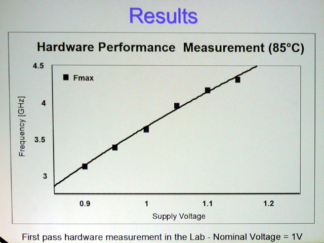
Xpirit disse:Só não acredito é nos 4-5Ghz de clock para o CELL em si. Os ***** 970FX vão em 2.5 Ghz. De 2.5 a 5 Ghz vai muito fruta.
O CELL talvez seja um Power a 2Ghz-2.5Ghz com 8 SPE's ao dobro da freq.
Acho que agora a curiosidade está nesse Power (O PPE nos slides) que está no Cell.
Deve ser uma versão cortado do Power5, mas ainda não deram pormenores.
A 2ª parte do artigo do Ars vai incluir os pormenores desse *****.
Tomorrow, after the next CELL session, I'll cover more of the Cell's basic architecture, including the mysterious 64-bit ***** core that forms the "brains" of this design.
4-5 Ghz para este core também me parece impossivel.