Computex (NV45+X600+X800PciEx+Intel 9xx+Board 754 e 939+bla bla bla)

Nemesis11

Power Member
IMG_6187_small.jpg


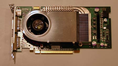
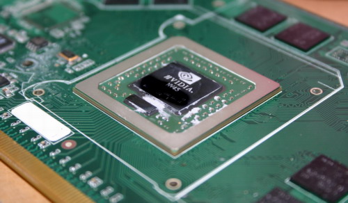
The surprise of the show was a brief encounter with NVIDIA's upcoming NV45, NVIDIA's PCI Express successor to the strong performing NV40 (GeForce 6800 Ultra).
At first glance, the NV45 card looks like a normal 2-slot NVIDIA graphics card
Upon closer look you'll notice that this particular card has a PCI Express x16 interface, but with no bridge chip. It looks like the rumors of a bridgeless NV45 were true.
Here's what we do know about NV45, it's currently running at a 450MHz core clock with 1.1GHz GDDR3 memory; this particular card uses Samsung chips. The 450MHz clock speed is a 12.5% increase in core clock speed over the GeForce 6800 Ultra, with memory speed remaining unchanged.

gigabyte_x600xt_small.jpg


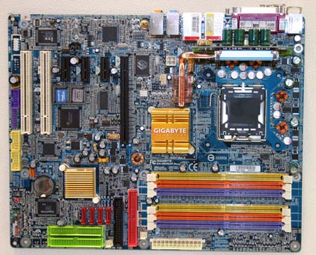
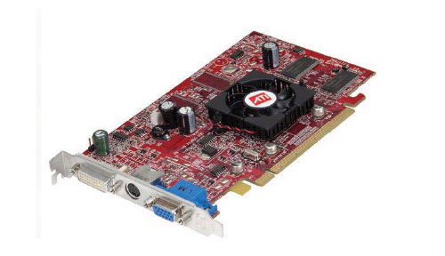
ATI had PCI Express boards spread out all over the show floor, with the PCI Express Radeon X600 XT showing up at Gigabyte's booth:
The X600 XT is basically a PCI Express version of the Radeon 9600XT with a higher memory clock (740MHz vs. 600MHz). We will have more details on the X600 in an upcoming article.
ASUS also had a X600 XT solution at their booth

IMG_6085_small.jpg


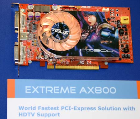
As well as a dual-DVI PCI Express X800 card
Remember that the PCI Express X800 is based off of a slightly different chip than the AGP X800, known internally as the R423 (R420 is the AGP version).

IMG_6089_small.jpg


The majority of the problems seem to reside with the 925X and its support for DDR2 memory, which has been through numerous revisions.We believe that the 925X being shown off at Computex is the fourth incarnation of the chip, which is pretty bad for Intel, especially considering that even in its current revision the chipset does not support ECC - a planned feature for the chipset.

The other complaints we've been hearing about from motherboard manufacturers involves Intel's LGA-775 socket. Since the pins have been moved off of the CPU and onto the socket itself with the LGA-775 interface, motherboard manufacturers have been reporting extremely high failure rates with those sockets. The pins on the socket itself are spring-loaded, and installing a CPU obviously causes the springs to compress. What seems to be happening however is that after a handful of CPU installations, the springs don't want to spring back to their original position - resulting in premature socket failures. The problem does seem to be a solvable one, but we'll have to wait and see what the motherboards we get our hands on are like. You better believe that we'll be testing socket reliability as soon as we get LGA-775 boards and CPUs in house.

asrock_dual_p4_small.jpg


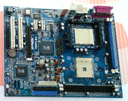
ASRock is displaying an interesting board that caught our eyes; the K8 Combo board features both a Socket-939 and a Socket-754 socket. Astute AnandTech readers will know that Socket-754 Athlon 64s only have one Hyper Transport link and thus cannot support multiple processors, so something must be up. Indeed the K8 Combo isn't a multiprocessor board, rather its a motherboard that can support either a Socket-939 CPU or a Socket-754 CPU, but not both. The flexibility offered by the board is interesting, as it provides a decent upgrade path for current Socket-754 users, granted it may be a bit extreme.

Muito mais aqui (http://www.anandtech.com/printarticle.html?i=2064). QBM, BTX, etc etc.

Have big fun.....
 
Última edição:
Essa socket da Intel, ca para mim sao os eng da Intel que nao devem ter mais nada que fazer .. entao bora la .. e que tal se tirarmos os pinos do cpu e os metermos na socket? Parece bem? OHHHHHHHHHHHHHHHHHHH sff .. keremos um prototipo para amanha ..
 
Bem essa AsRock supreendeu-me e lembra-me dos velhos tempos das mobos manhosas com slot1 e socket370, agora a questão é saber se é bem implementado e qual a performance ;)
 
Fiquei agradavelmente surpreendido por ver tanta preocupação em fazer mobos de transição com AGP e PCIEx, DDR2 e DDR, e até a chegar ao impensável s754 e s939! 8o

Finalmente puseram os pés na terra e perceberam que a malta não está disposta a trocar tudo dentro do PC de uma vez só! :cool:
 
Então a nVidia decidiu mesmo chamar NV45 à NV40 com PCI express?
Sendo assim parece que desistiram de usar o bridge (pelo menos com a 6800 Ultra).


A X600 é mesmo uma RV350... :(
No entanto a 740 Mhz (com aquele cooler minusculo?! )pode ser que se vejam umas surpresas.. metam-lhe uma largura de banda de 256bits e um overclock de 100Mhz e temos uma placa à maneira :D
 
ToTTenTranz disse:
Então a nVidia decidiu mesmo chamar NV45 à NV40 com PCI express?
Sendo assim parece que desistiram de usar o bridge (pelo menos com a 6800 Ultra).

Eles podem ter uma solução com bridge e outra sem.
Agora falta saber onde é que eles vão usar o HSI. Se era só para as PCX, não faz muito sentido. Talvez seja só para as placas low-end.
Na Hexus indicavam que podia existir uma HSI ao contrario para que placas PciEx funcionassem em Agp.
Uma coisa é certa, aquilo só tem uma molex.

ToTTenTranz disse:
A X600 é mesmo uma RV350... :(
No entanto a 740 Mhz (com aquele cooler minusculo?! )pode ser que se vejam umas surpresas.. metam-lhe uma largura de banda de 256bits e um overclock de 100Mhz e temos uma placa à maneira :D

740 é as mems :D. 500 de core. Isto deve ser 128 bit de bus. Mas a noticia não tras nada.
O Inq diz que a X300 é 128 bit e a X300SE é 64 bit (WOW!!! lol). Mas nada sobre a X600.
http://www.theinquirer.net/?article=16227

Mais umas coisas. O Anando diz que não viu nada do BTX e critica um pouco a Intel. Outra coisa é o picoBTX, que me pareceu muito grande e com espaço só para 1 agp ou 1 pci.
 
Alguém me sabe dizer qual é o aumento de performance do pci-e em relação ao agp???


e no caso especifico da 6800, de quanto é o ganho do pci-e??


....e já agora - os ganhos de performance são relativamente iguais, entre a nvidia e a ati?
 
[JoaoR] disse:
Alguém me sabe dizer qual é o aumento de performance do pci-e em relação ao agp???


e no caso especifico da 6800, de quanto é o ganho do pci-e??


....e já agora - os ganhos de performance são relativamente iguais, entre a nvidia e a ati?

Que eu saiba não se sabe os ganhos (se é que há ganhos na pratica). O que parecia é que a nVidia perdia performance com o HSI bridge, mas este 6800 já não o tem.
Tem que se esperar pelos benchs.
 
humm, pois o suporte nativo do pci-e por parte da nvidia, é realmente uma boa jogada da nvidia dadas as criticas que estavam a ser feitas ao chip bridge que íam supostamente usar. só resta saber os ganhos reais do pci!?!?


thanks nemesis ;)
 
Cambada de xulos! Espero k haja boards com AGP, PCIx e slots Pci...
Desculpem a minha ignorância, mas k slots pekenos pretos são akeles na board da gigabyte? É algum slot AMR (k tb nunca soube pa k servia sinceramente)?
 
SteelBoy19 disse:
Cambada de xulos! Espero k haja boards com AGP, PCIx e slots Pci...
Desde que não vás para um ***** intel, não tens problemas (há pelo menos Via e Sis). Tb há umas MSI com ***** 865 e socket 775 (é sempre uma hipotese para fugir ao Pci Ex 16X)

SteelBoy19 disse:
Desculpem a minha ignorância, mas k slots pekenos pretos são akeles na board da gigabyte? É algum slot AMR (k tb nunca soube pa k servia sinceramente)?

Pci Express 1X
 
Uns updates nVidia + Ati

Bem.....parece que o Anando meteu os pés pelas mãos em relação à NV45

bridge.jpg


O HSI continua lá, mas mais "escondido". Os clocks nesta board de testes tb estão reduzidos.

First of all, it seems that at least some of the samples of NV45 that NVIDIA handed out are running at 350MHz with 1GHz GDDR3 memory, which is slower than the current NV40 GPU.

The second, smaller die is NVIDIA's High Speed Interconnect (HSI) which is an AGP-to-PCI Express bridge, meaning that NV45 is still an AGP part

powerconnector.jpg


Uma ligação de power misteriosa. A tal ligação em que seria preciso uma segunda fonte.

+ em http://www.anandtech.com/printarticle.html?i=2067

---------------------------------------------------------------

x300.png

X300 em 0.11nm. É uma 9200 ou uma 9600 com clocks reduzidos. Não dá para perceber bem.

In the same way that ATI moved into the 130nm low-k process with the 9600 line of cards, the RV370 GPU of the X300 will be fabbed on a 110nm process. As usual, TSMC is behind the silicon process that ATI is using.

It's good to see ATI sticking with a strategy that has worked for them. Taking an aggressive chance on one line of mid-range or low end GPUs before moving the rest of the parts to another process is a very good way to work out the kinks without incurring too much risk. In the worst case scenario, ATI could have covered the market segment with a lower clocked or otherwise handicapped version of a higher performing part while fixing what went wrong. What we have seen in the past with NVIDIA and large CPU vendors has consisted of large scale shifts in process technology, which can really hurt production and/or time to market if something goes wrong.

Among the benefits that ATI cites in TSMC's 110nm process is the ability to fit 40% more transistors in the same area as 130nm. A straight die shrink only accounts for about a 30% increase in space efficiency (1 - 1102 / 1302), so it stands to reason that TSMC must have made up the space savings in other areas of their process technology. Either way, this means that ATI has a lot of headroom with what they want to do with RV370.

Of course, with any new process, yeilds will be lower than what would be desired for the same performance level on an established process. Our theory is that ATI has worked out a way around this issue by taking the RV360 (Radeon 9600) core with a few tweaks, and fabbed it on a 110nm process, and dropped the clock speed way down in order to achieve acceptable yeilds. We can't be sure about this, as ATI isn't going to share yield rates or if this is actually a reason why they have taken this route. The pieces just seem to fit together too well, but it's still possible that it's all just coincidence.

The RV370 GPU will eventually be marketed as two parts: the Radeon X300 and the Radeon X300 SE. The SE part will have the same features as the 9200 SE - a cut-down 64bit memory interface. This value segment part will perform better than the 9200 SE part both because its based on the RV360 core, and its a higher clocked part. Hopefully, this also means that the compatibility issues we saw with the 9200 parts will fade into the distance as well. The regular X300 will have a 128bit memory interface.

Mais sobre a X800, X600, X300, Mobility X600 e Axiom:
http://www.anandtech.com/printarticle.html?i=2066
 
Última edição:
Nemesis11 disse:
740 é as mems :D. 500 de core. Isto deve ser 128 bit de bus. Mas a noticia não tras nada.
O Inq diz que a X300 é 128 bit e a X300SE é 64 bit (WOW!!! lol). Mas nada sobre a X600.
http://www.theinquirer.net/?article=16227

Pois é.. oops.. então a X600 é uma valente merd@... O core é o mesmo da 9600XT portanto o fillrate tambem é..
As placas de gama média alta da nvidia já usam gddr3 a 1ghz.. Se o RV350 usasse memória dessa velocidade ia ser muito mais rápido.. enfim...
 
Será que o Pci Express vai ser uma banhada?

Retirado do Anando

Question 2: When is NV45 being released?

We've heard two different things from manufacturers. Some manufacturers have told us that NV45 will be available in August, while others have basically said that NV45 won't be out this year, instead we will see NV48 arrive as an AGP refresh to NV40 by Christmas.

What will most likely happen is that NVIDIA will determine the fate of NV45 by the acceptance (or lack thereof) of PCI Express this year. If the acceptance is low enough, NV45 will be pushed out to next year, otherwise we may see it in Q3/Q4. Regardless of what happens, it does seem like NV48 will be NVIDIA's fall refresh product, and that will be an AGP solution.

A Ati parece toda apostada no pci Ex, mas a nVidia nem por isso.
 
tendo em conta os fabulastiscos ganhos de performance que fomos tendo entre as varias iteraçoes do AGP realmente nao sei se espero grande coisa do PCI-E... Mas a diferença teorica e consideravel pode ser... Mas os fabricantes continuam a apostar em maximizar a RAM da grafica. Enquanto chegar para um jogo e nao tiver de fazer trocas com a memoria principal provavelmente ate o PCI-E extra 2 versao especial de corrida nao vai servir para grande coisa..
mas a evolução ta sempre ai e a nvidia devia-se deixar de *****s e aderir ao PCI-E. quantas vezes e que a necessidade aparece depois da coisa que a resolve?
 
Cheira-me que a XT platinum foi uma grafica para reviews e para fazer uma edição muito limitada.

Preview do Pci Ex das Ati ( http://techreport.com/etc/2004q2/ati-pcie/index.x?pg=1 )

For starters, there is no direct PCI Express equivalent to the Radeon X800 XT Platinum Edition. ATI expects the first wave of PCI Express orders to be from OEMs, and the Platinum Edition is a little extreme for the likes of Dell. A PCI Express Radeon X800 XT will be available, though, just with a little less bling than the Platinum Edition.

E depois fica um enorme buraco entra a X800pro e a X600XT, que a Ati vai ter que preencher

Despite claims that its X800 architecture scales down to eight- and four-pipe designs, the low end of ATI's PCI Express Radeon X-series is dominated by last year's technology. Not that there's anything wrong with last year's technology, though. The X600 and X300's RV360 roots leverage a proven rendering pipeline, full 24 bits of pixel shader precision, and the most gorgeous antialiasing around.

Other than PCI Express support and a slight memory clock boost for the XT, the X600 line doesn't offer much over ATI's existing Radeon 9600 series products. However, the X300 is a significant improvement over ATI's previous value workhorse, the DirectX 8-class Radeon 9200 series. ATI expects the Radeon X300s to be twice as fast as the 9200s, which is a pretty significant leap when you add DirectX 9-class shaders to the equation.

------------------

EDIT: Afinal as 915 tb podem ter Agp

computex04_ecsboard.jpg


http://www.theinquirer.net/?article=16262
 
Última edição:
Back
Topo