
You are using an out of date browser. It may not display this or other websites correctly.
You should upgrade or use an alternative browser.
You should upgrade or use an alternative browser.
Processador Curiosidades de hardware
- Autor do tópico Nemesis11
- Data Início
Nemesis11
Power Member
A Google Japan criou um teclado inovador e mais fácil de utilizar, só com 1 Row. Tem 165 cm de comprimento, mas apenas uns milimetros de altura.
Pode ser usado de forma colaborativa e, além disso, pode ser utilizado noutras funções.


Layout:

Video:
https://github.com/google/mozc-devices/tree/master/mozc-bar
Pode ser usado de forma colaborativa e, além disso, pode ser utilizado noutras funções.
Layout:
Video:
https://github.com/google/mozc-devices/tree/master/mozc-bar
Última edição:
Sim, durou muito pouco tempo (até a AMD ter comprado a NexGen).Não durou assim tão pouco tempo porque o AMD K6 é o Nx686.

Novo Vector Engine da NEC

CORES, CLOCKS, AND CACHES CRANKED WITH LATEST NEC VECTOR ENGINES
First, let’s take a look at the NEC Aurora accelerator roadmap:
Generally speaking, NEC has been focused on growing the memory bandwidth with each generation and scaling out the compute capacity as it can. With the VE30 generation, expected about now in 2022, the roadmap promise was to deliver more than 2 TB/sec of memory bandwidth on each device, which is up there with the latest GPU accelerators on the market used for HPC and AI workloads. To be specific, the NEC roadmap called for the VE30 to have a “new architecture, larger memory bandwidth, higher core count, higher frequency, and new functions.”
Here is what we know. The number of cores in the VE30 is 16, compared to the 10 cores in the VE20, and the memory bandwidth has increased by 1.6X and the memory capacity has increased by 2X. If you do the math on all of that, then the 16 core VE30 vector math accelerator has 96 GB of HBM2e memory (we presume NEC has not made an aggressive move to HBM3 like Nvidia has and is saving that for the VE40 upgrade coming next year) and has 2.45 GB/sec of aggregate bandwidth coming out of that HBM2e memory
While NEC did not specify any of this, we think it has shifted from a 16 nanometer process from Taiwan Semiconductor Manufacturing Co used with the VE10 and VE20 accelerators in the Aurora family to a reasonably mature 7 nanometer process from TSMC.
The other bit of data we know is that Tohoku University in Japan, is going to take delivery of a supercomputer stuffed with 4,032 of these VE30 engines that is expected to be rated at around 21 petaflops of peak aggregate floating point compute at 64-bit precision.
https://www.nextplatform.com/2022/1...aches-cranked-with-latest-nec-vector-engines/If you do the math backwards on that, then a 16-core VE30 vector accelerator is rated at 5,208 gigaflops, and that means the peak FP64 performance per core on the VE30 is 325.5 gigaflops. That’s a tiny bit less than a 6 percent increase in per-core performance compared to the core in a VE20 vector accelerator. Which means the clock speed on the VE30 is only that 6 percent higher than the 1.6 GHz of the VE20
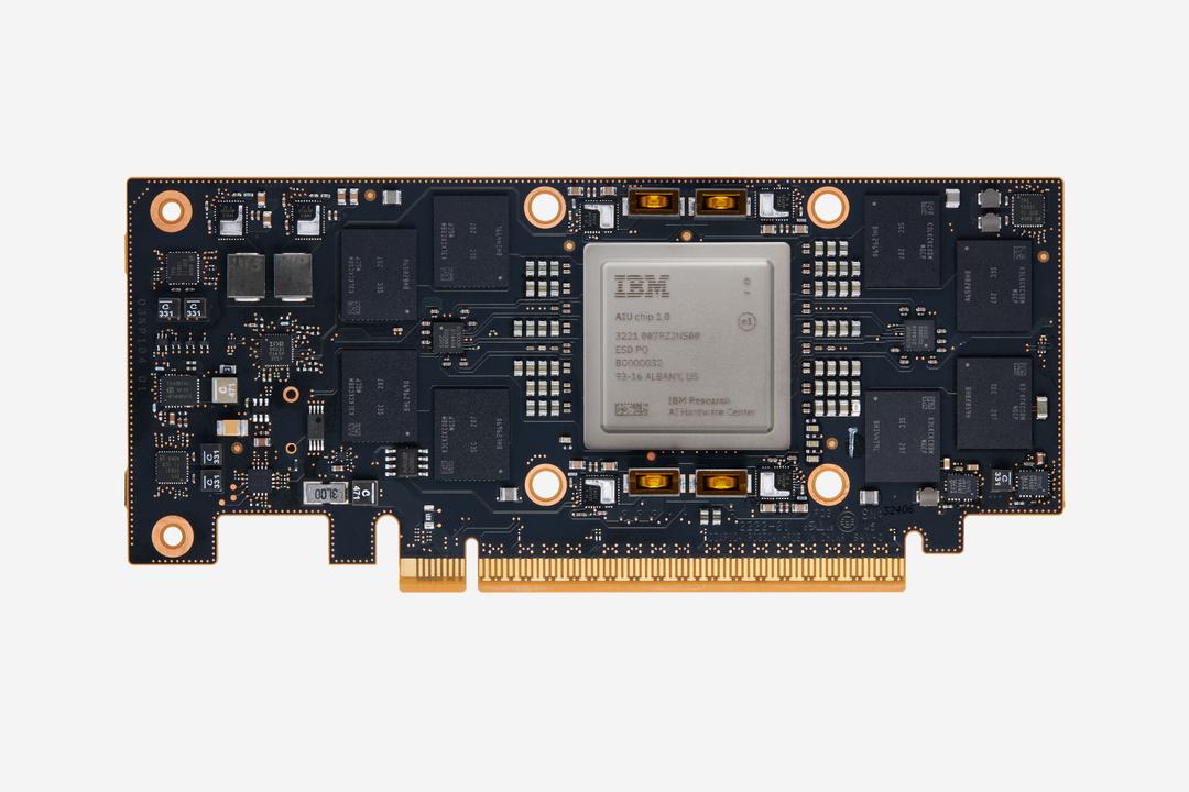
Meet the IBM Artificial Intelligence Unit
The workhorse of traditional computing — standard chips known as CPUs, or central processing units — were designed before the revolution in deep learning, a form of machine learning that makes predictions based on statistical patterns in big data sets. The flexibility and high precision of CPUs are well suited for general-purpose software applications. But those winning qualities put them at a disadvantage when it comes to training and running deep learning models which require massively parallel AI operations.
For the last decade, we’ve run deep learning models on CPUs and GPUs — graphics processors designed to render images for video games —when what we really needed was an all-purpose chip optimized for the types of matrix and vector multiplication operations used for deep learning. At IBM, we’ve spent the last five years figuring out how to design a chip customized for the statistics of modern AI.
In our view, there are two main paths to get there.
One, embrace lower precision. An AI chip doesn’t have to be as ultra-precise as a CPU. We’re not calculating trajectories for landing a spacecraft on the moon or estimating the number of hairs on a cat. We’re making predictions and decisions that don’t require anything close to that granular resolution.
With a technique pioneered by IBM called approximate computing, we can drop from 32-bit floating point arithmetic to bit-formats holding a quarter as much information. This simplified format dramatically cuts the amount of number crunching needed to train and run an AI model, without sacrificing accuracy.
Leaner bit formats also reduce another drag on speed: moving data to and from memory. Our AIU uses a range of smaller bit formats, including both floating point and integer representations, to make running an AI model far less memory intensive.
Two, an AI chip should be laid out to streamline AI workflows. Because most AI calculations involve matrix and vector multiplication, our chip architecture features a simpler layout than a multi-purpose CPU. The IBM AIU has also been designed to send data directly from one compute engine to the next, creating enormous energy savings.
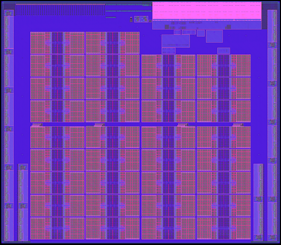
https://research.ibm.com/blog/ibm-artificial-intelligence-unit-aiuThe IBM AIU is what’s known as an application-specific integrated circuit (ASIC). It’s designed for deep learning and can be programmed to run any type of deep-learning task, whether that’s processing spoken language or words and images on a screen. Our complete system-on-chip features 32 processing cores and contains 23 billion transistors — roughly the same number packed into our z16 chip. The IBM AIU is also designed to be as easy-to-use as a graphics card. It can be plugged into any computer or server with a PCIe slot.
This is not a chip we designed entirely from scratch. Rather, it’s the scaled version of an already proven AI accelerator built into our Telum chip. The 32 cores in the IBM AIU closely resemble the AI core embedded in the Telum chip that powers our latest IBM’s z16 system. (Telum uses transistors that are 7 nm in size while our AIU will feature faster, even smaller 5 nm transistors.)
Diria que nenhum dado que é um processador específico para AI, e como tal apenas retira partido de SW específico. Isto no fundo não é muito diferente de outro tipo de "aceleradores" usados nos PCI-e.
Mais para trás há aí uma série de chips/SoC de start ups que estão a pensar fora da caixa, tal como neste caso a IBM, construindo de raiz chips específicos para AI e ML, em que os ganhos são significativos.
Mais para trás há aí uma série de chips/SoC de start ups que estão a pensar fora da caixa, tal como neste caso a IBM, construindo de raiz chips específicos para AI e ML, em que os ganhos são significativos.
Nemesis11
Power Member


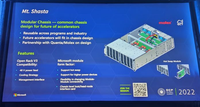
Uma coisa curiosa que a Microsoft e a Quanta apresentaram na OCP Summit
Microsoft QCT Mt Shasta Platform for FPGA and ASIC Farms at OCP Summit 2022
Microsoft is heavily invested in FPGAs and ASICs. At the same time, it faces a practical problem. Putting a FGPA or ASIC in a PCIe slot limits the power and cooling available for these devices while at the same time increasing heat generation in traditional servers. As such, Microsoft tapped QCT and Molex to build the new OCP Mt Shasta Platform to house its growing farm of accelerators.
Microsoft’s Open Rack V3 chassis takes 48V bus bar input power input and has shared cooling for up to eight accelerator blades. Using this setup, Microsoft is able to deliver power and cooling to high-power devices. It also features hot-swap capabilities and the ability to have flexible device connectivity.
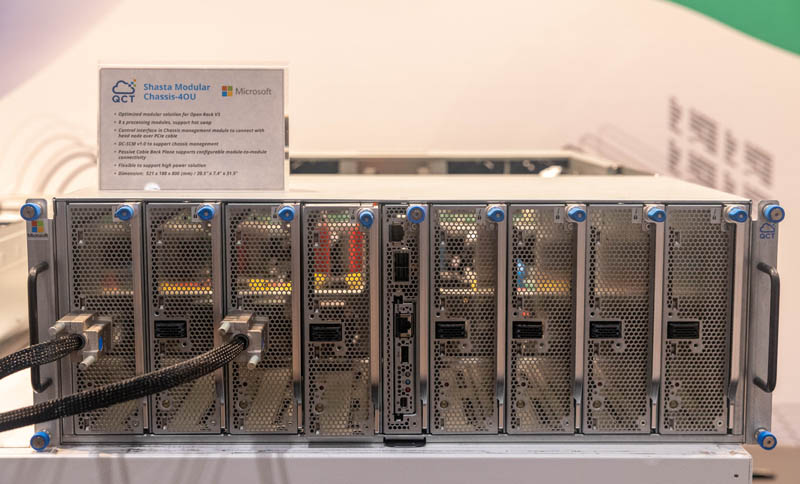
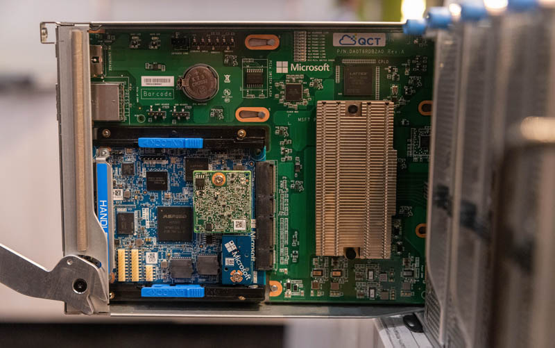
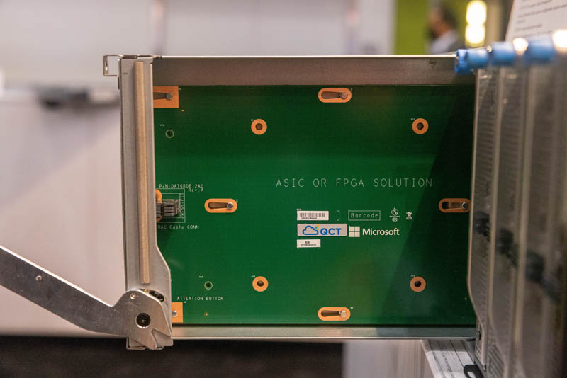
One of the features one will immediately notice is that there are external DACs made by Molex.
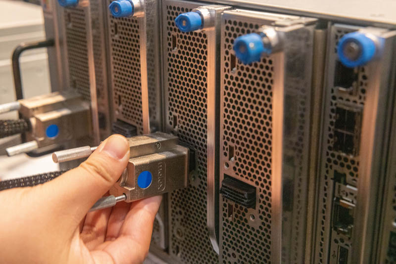
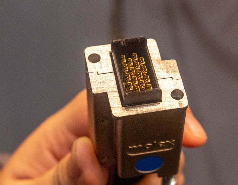
The back of these blades has the mating parts as well as cables between the management module and the individual FPGAs. Instead of a PCB backplane, Microsoft is using a cabled backplane here.
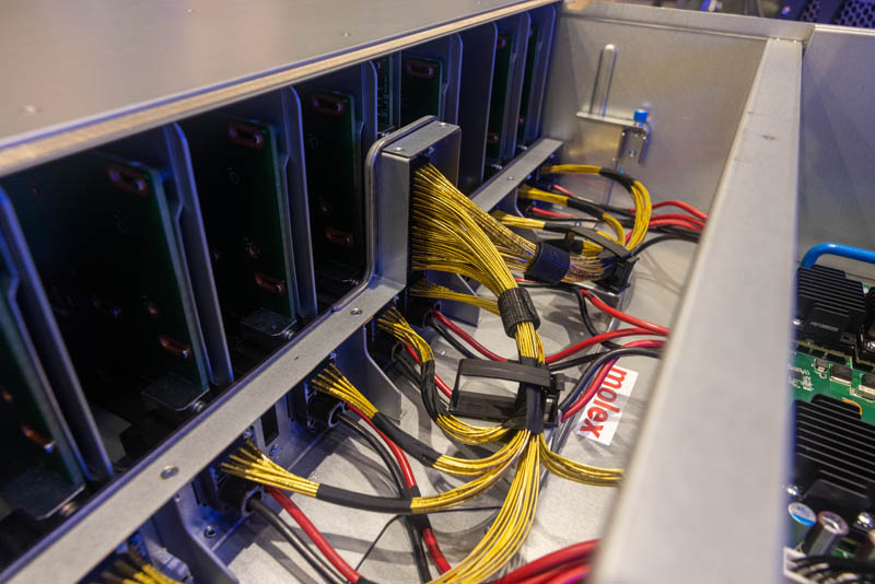
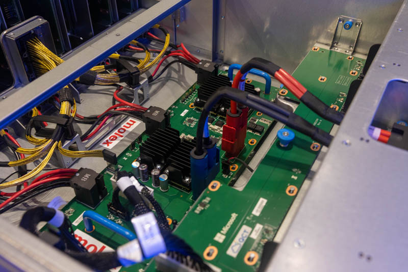
https://www.servethehome.com/micros...m-for-fpga-and-asic-farms-at-ocp-summit-2022/Overall, the Microsoft/ QCT Mt Shasta/ Shasta chassis is interesting. Microsoft told us that the reason it is not using OAM as a PCIe alternative or EDSFF E3 is that it needs higher power and hot swap capability. OAM offers power, but not hot-swap. E3 offers hot swap, but not high power. PCIe slots offer neither hot swap nor high power operation.
Nemesis11
Power Member
A Broadcom mostrou um package com a o Tomahawk 4 incorporando Optics e outro Photonics,incorporados com o Chip, que são bem interessantes.
")


https://www.servethehome.com/awesom...optics-and-silicon-photonics-ocp-summit-2022/
Ainda devem estar para sair mais uns quantos, NVIDIA, Marvell, etc

Wt...
Não me recordo de alguma vez ter visto uma coisa destas
Não me recordo de alguma vez ter visto uma coisa destas
Por acaso já tinha visto um à venda no OLX e um rádio também.Wt...
Não me recordo de alguma vez ter visto uma coisa destas
Nemesis11
Power Member
Water Cooling e Cooling por imersão para soluções com aceleradores, de 8 kW de TDP (8 x 1 kW).
Water cooling:


Imersão:

Acho muito interessante as soluções que vão aparecendo de cooling, para o enorme aumento que tem existido a nível de TDPs.
Bonus.
Chassis com 24 aceleradores no formato M.2 ou 12 no formato "Dual" M.2:

https://www.servethehome.com/wiwynn...ling-solution-at-ocp-summit-2022-liquidstack/
Water cooling:
Imersão:
Acho muito interessante as soluções que vão aparecendo de cooling, para o enorme aumento que tem existido a nível de TDPs.
Bonus.
Chassis com 24 aceleradores no formato M.2 ou 12 no formato "Dual" M.2:
https://www.servethehome.com/wiwynn...ling-solution-at-ocp-summit-2022-liquidstack/
EDIT:
Aqui nas anotações está invertido, o iGPU está do lado direito

Última edição: