
vitorbruno89
Power Member
NVIDIA GeForce GTX 580/570 (GF110)
AMD is undertaking its product development cycle at a breakneck pace, NVIDIAtrailed it in the DirectX 11 and performance leadership race by months. This November, AMD will release the "Cayman" GPU, its newest high end GPU, the expectations are that it will outperform the NVIDIA GF100, that is a serious cause for concern, for the green team. It's back to its old tactics of talking about GPUs that haven't even taken shape, to try and water down AMD's launch. Enter, the GF110, NVIDIA's new high-end GPU under design, on which is based the GeForce
The new GPU is speculated to have 512 CUDA cores, 128 TMUs, and a 512-bit wide GDDR5 memory interface holding 2 GB of memory, with a TDP of close to that of the GeForce GTX 480. In the immediate future, there are prospects of a more realistic-sounding GF100b, which is basically GF100 with all its 512 CUDA cores enabled, while retaining its 384-bit GDDR5 memory interface, 64 TMUs, and slightly higher TDP than that of the GTX 480.
In TechPowerUp
A Fixed Fermi Core Called GF110 Goes Into GTX580!
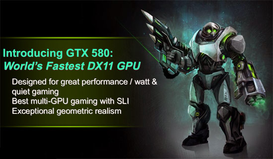
This morning NVIDIA has finally introduced the GeForce GTX 580 video card after many weeks of rumors and information leaks. It has only been seven months since NVIDIA released the GeForce GTX 480 video card, but that card is officially no longer the flagship GPU of the NVIDIA arsenal. Priced at $499, the GeForce GTX 580 comes at the same suggested retail price as the GeForce GTX 480 did, but the video card has higher clock speeds and all 512 CUDA cores enabled thanks to a new GPU die revision.
NVIDIA has essentially gone back to the drawing board with their Fermi GF100 GPU and has re-engineered it at the transistor level. Through this redesign the company was able to turn up the clock speed with less power usage since they were able to see what worked well and what didn't work at all in the original GF100 GPU. The result of their efforts is now called the GF110 and that is what we will be taking a closer look at today. The GPU is still made by TSMC on their 40nm process technology, but you'll see it is a while new beast!
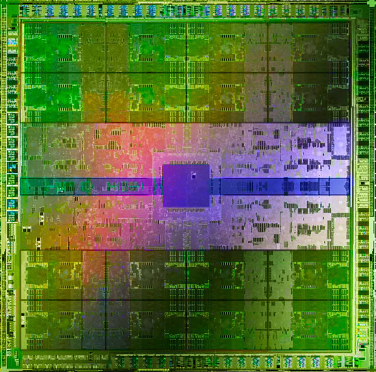
What is new with the GF110 on the GeForce GTX 580? If you look at the block diagram above you won't see any changes as NVIDIA did not issue a new diagram since the original GF100 die shot that you can see above. NVIDIA told us that the GF110 has roughly 3.05 Billion transistors and that the GF100 has 3.01 Billion transistors and the overall die size remains the same. You might be wondering how this could be true since the GeForce GTX 580 has more CUDA Cores, texture units and SMs than the GeForce GTX 480. Well, the simple answer there is that NVIDIA had to disable part of the GF100 GPU core in order to launch the GTX 480 product in a somewhat timely manner. While NVIDIA was 'under the hood' making performance and power improvements they did add two new elements that are worth pointing out. The first is that the GeForce GTX 580 now supports full-speed FP16 texture filtering. NVIDIA said that this will help performance in certain texture-heavy applications. Second, the GeForce GTX 580 also supports new tile formats that improve Z-cull efficiency.
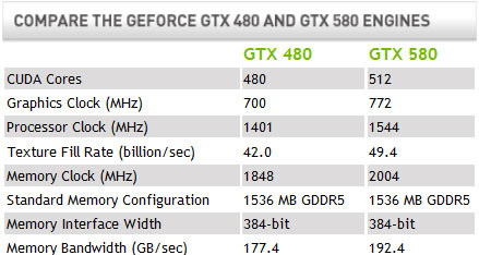
NVIDIA said that these clock-for-clock enhancements increase the GTX 580's performance versus the GTX 480 by anywhere from 5-14% depending on the benchmark.
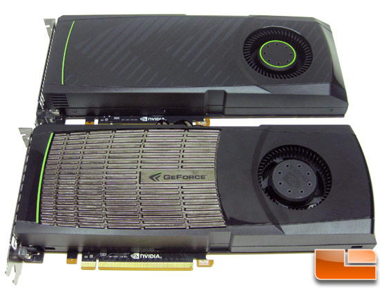
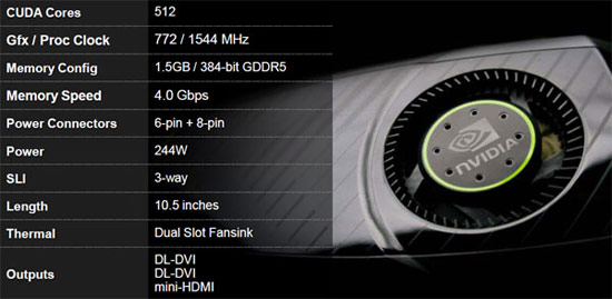
The thing is that the GeForce GTX 580 doesn't run at the same clock speed; the GTX 580 runs at higher clock speeds! The GeForce GTX 480 had a GPU clock of 700MHz, a Stream Processor clock of 1401MHz and the 1536MB frame buffer consisting of Samsung GDDR5 memory was clocked at 924MHz, for an effective data rate of 3696MHz. The GeForce GTX 580 has a GPU core clock speed of 772MHz, a Stream Processor clock of 1544MHz and the 1536MB GDDR5 memory is now running at 1002MHz, for an effective data rate of 4008MHz. Looking at the picture above you can see the GeForce GTX 480 sitting below the new GeForce GTX 580. Visually the two cards are very different looking and this is thanks to the improvements on the GF110 Fermi core. The GeForce GTX 580 runs cooler and uses less power despite the fact that it runs at a core clock speed that is 10.3% faster than the GTX 480!
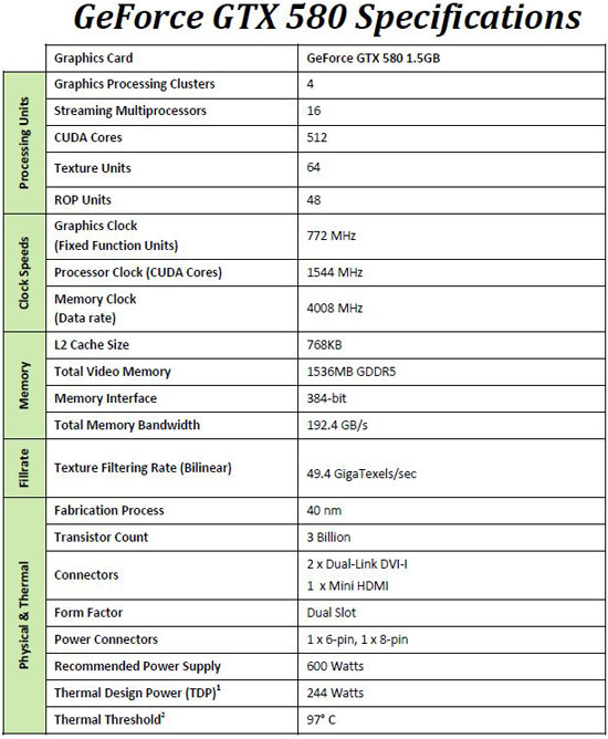
Many of our readers love specification charts and here is a good one that NVIDIA provided that shows what the GTX580 has to offer. The Thermal Design Power went from 250 Watts on the GTX 480 down to 244 Watts on the GTX 580.
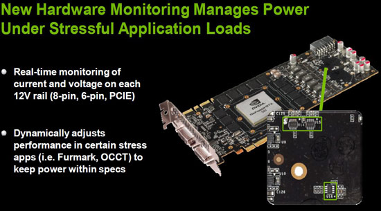
One of the most interesting new features on the GeForce GTX 580 that we need to talk about is the new power monitoring hardware that is on the GTX 580. Beginning with the GTX 580 we are told that NVIDIA will include dedicated hardware circuitry on the graphics card that performs real-time monitoring of current and voltage on each 12V rail (6-pin, 8-pin and the PCI Express slot itself). Code in the video card driver then monitors these power levels and then will dynamically adjust performance in certain stress applications such as Furmark or OCCT. This will keep the board from having excessive power draw. NVIDIA will have to now keep drivers updated and track how certain games or applications stress the GPU.
Review's by LogitechReview:
-> Full Review by LogitReview GTX 580
-> NVIDIA GeForce GTX 580 SLI Benchmarking with ASUS ENGTX580
Unboxing by Linus Tech Tips:
-> EVGA NVIDIA GeForce GTX 580 1.5GB
NVIDIA GeForce GTX 570 1.25GB
When we got an overnight package from NVIDIA this past Friday we expected it to be a holiday gift like most of the other companies are doing right now. We've been loaded up with holiday cookies and greeting cards so far this month, so when we got the above package from NVIDIA it looked to be a holiday surprise.

Once we opened up the package we found a holiday card and a welcome letter letting us know that we were given the NVIDIA GeForce GTX 570 reference card to review and that the official launch date was December 7th, 2010 at 6am PST. NVIDIA gave us just over three days to review the GeForce GTX 570; how nice of them. NVIDIA must guess that hardware reviewers do nothing over the weekend or they wanted to slip something past reviewers that they didn't want discovered. In our 'holiday gift box' we got a reviewer's guide, a GeForce GTX Tank T-Shirt: Collector's Edition and a single GeForce GTX 570 reference card.
As many of our readers knew already, the new NVIDIA GeForce GTX 570 uses the same GF110 Fermi core that is found on the GTX 580 but it has a number of things disabled. If you look at the specifications chart below you'll see that the GeForce GTX 570 has fewer SMPs, CUDA Cores, Texture Units, ROP Units, GDDR5 memory and lower overall performance than the GeForce GTX 580.
As you can see the GeForce GTX 570 has 480 CUDA cores and 15 PolyMorph engines. If you recall this is pretty much the same processing unit configuration as the original GeForce GTX 480 as it too had 480 CUDA Cores and 15 PolyMorph engines. The GeForce GTX 480 had a GPU clock of 700MHz, a Stream Processor clock of 1401MHz and the 1536MB frame buffer consisting of Samsung GDDR5 memory was clocked at 924MHz, for an effective data rate of 3696MHz. The new GeForce GTX 570 has a GPU core clock speed of 732MHz, a Stream Processor clock of 1464MHz and the 1280MB (1.25GB) GDDR5 memory is now running at 950MHz, for an effective data rate of 3800MHz. The GeForce GTX 570 runs faster on the core since it has higher clock speeds, but the memory bandwidth is 14% less than the GeForce GTX 480 (177.4GB/s) since it has less memory and operates on a narrower 320-bit bus. That means the GeForce GTX 570 should perform better in applications where it is not being memory limited.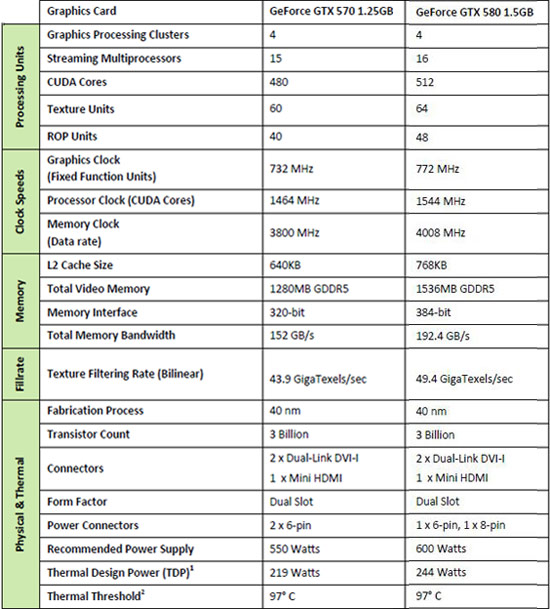

Since the GeForce GTX 570 is so close to the GeForce GTX 480 it makes no since to continue to carry both video cards. NVIDIA confirmed that now that the GTX 570 GPU has been released that the GeForce GTX 480 will be discontinued after the supply of chips/cards runs out. Both the NVIDIA GeForce GTX 480 and GTX 465 are End of Life (EOL). The GeForce GTX 470 will remain in the product stack at $254.99 with the GeForce GTX 570 at $349.99 and the GeForce GTX 580 at $509.99. With the ATI Radeon HD 5870 coming in at $259.99 the GeForce GTX 570 doesn't have any direct price competition until AMD released their Cayman series of video cards which will consist of the Radeon HD 6970 and 6950 and that is supposed to happen next week. Let's take a closer look at the GeForce GTX 570 and see what it is all about!
Review's:
-> NVIDIA GeForce GTX 570 1.25GB Video Card Review by LogitechReview
-> GeForce GTX 570 SLI Review by Guru3d
Unboxing by Linus Tech Tips:
-> EVGA NVIDIA GeForce GTX 570
Última edição:
")