TSMC 3nm - 2022

Rafx

Power Member
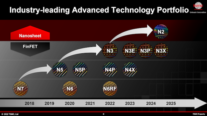
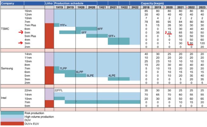
Ontem foi falado que os 5nm da TSMC estarão em produção em 2020, hoje é anunciado que os 3nm estarão prontos a produzir em 2022, um ano antes do projectado inicialmente (2023).

Esta noticia segue-se também ao facto da TSMC se ter tornado a empresa asiática mais valiosa, ultrapassando gigantes como a Samsung.

TSMC is delivering record results day after day, with a 5 nm manufacturing process starting High Volume Manufacturing (HVM) in Q2 next year, 7 nm process getting plenty of orders and the fact that TSMC just became the biggest company publicly trading in Asia. Continuing with the goal to match or even beat the famous Moore's Law, TSMC is already planning for future 3 nm node manufacturing, promised to start HVM as soon as 2022 arrives, according to JK Wang, TSMC's senior vice president of fab operations. Delivering 3 nm a whole year before originally planned in 2023, TSMC is working hard, with fab construction work doing quite well, judging by all the news that the company is releasing recently.

We can hope to see the first wave of products built using 3 nm manufacturing process sometime around end of year 2022, when the holiday season arrives. Usual customers like Apple and HiSilicon will surely utilize the new node and deliver their smartphones with 3 nm processors inside as soon as the process is ready for HVM.
fonte

Se suceder como foi com os 7nm e como deve suceder com os 5nm, a AMD apresentará cpu's (Zen 6?) 3nm em 2023.
Para a AMD a nível de cpus consumidor o calendário deve ser:
2020: Zen 3, a 7nm 'optimizados' (7nm+?), ainda socketAM4
2021: Zen 4, a 5nm (+novo socket e ddr5)
2022: Zen 5, serão 5nm+/melhorados(?)
2023: Zen 6, 3nm

Isto a manter a cadência planeada de cpu's e a tendencia de uso de novos processos de fabrico no ano seguinte à estreia dos mesmos para a Apple.

Mesmo não tendo a estreia/bleeding edge logo que os novos processos estão a produzir, a AMD consegue manter uma cadência...tick-tock.


Conseguindo a TSMC realmente adiantar os 3nm para 2022, só mais más noticias a escalar para o lado da Intel..
Relembro que a Intel só terá 7nm prontos para 2021, mas que em 2021 a 7nm para consumidor só irá haver os novos gpu's discrete, portanto os primeiros cpu's 7nm da Intel só para 2022 a concorrer directamente com os 3nm da TSMC que hoje se falou.
 
Última edição:
Edited Transcript of 2330.TW earnings conference call or presentation 16-Apr-20 6:00am GMT
Finally, I will talk about our N3 status. Our N3 technology development is on track, with risk production scheduled in 2021 and target volume production in second half of 2022. We have carefully evaluated all the different technology options for our N3 technology, and our decision is to continue to use FinFET transistor structure to deliver the best technology maturity, performance and costs. Our N3 technology will be another full node stride from our N5, with about a 70% larger density gain, 10 to 15% speed again and 25% to 30% power improvement as compared with N5. Our 3-nanometer technology will be the most advanced foundry technology in both PPA and transistor technology when it is introduced and will further extend our leadership position well into the future.
https://finance.yahoo.com/news/edited-transcript-2330-tw-earnings-161634209.html
 
Li que a densidade dos 3nm é 250milhões de transistores por mm2. Isso é equivalente aos transistores dos últimos P-4 (188M single core e 376M dual core)

O CCD do zen2 teria 15mm2 :D Se for escalar para o tamanho do CCD atual e arredondando para cima, temos 78mm2, 40 cores e 160 MB de Cache :D

Os cores/L3 do TR 3990X ia ocupar meros 125mm2, exactamente... o IOD do zen2 AMD :wow:

Não fico admirado que se os CCD zen6 saírem com 32 Cores, se bem que parece ser algo absurdo... Talvez fiquem pelos 16C e cada core tenha uma quantidade maior de transistores para aumentar o IPC.
 
Última edição:
2021/2022
Now the situation gets fuzzier, Intel’s 7nm process is due to start ramping in 2021 with a 2.0x shrink. Samsung and TSMC are both due to begin 3nm risk starts in 2021. Assuming Intel hits their date, they may briefly have a production density advantage but Intel’s 14nm and 10nm process have both been several years late. With COVID 19 impacting the semiconductor industry in general and the US in particular, a 2021 production date for Intel may be even less likely.

Figure 6 compares 2021/2022 processes assuming that within plus or minus a quarter or two all three processes will be available, I believe this is a fair assumption. Intel has said their density will be 2.0x 10nm, TSMC on their 2020-Q1 conference call said 3nm will be 70% denser than 5nm so presumably 1.7x, Samsung has said 3nm reduce the die size by 35% relative to 5nm and that equates to a approximately 1.54x denisty.
TSMC-Process-Lead-Slides-20200427_Page_6-768x432.jpg.webp

Some key observations from figure 6.

  1. The individual numbers in figure 6 are our estimates and may need to be revised as we get more information, but the overall process densities match what the companies have said and should be correct.
  2. In spite of being the first to move to HNS, Samsung’s 3nm is the least dense of the three processes. The early move to HNS may make it easier for Samsung to shrink in the future but for their 3nm node isn’t providing the density advantage that you might expect from HNS.
  3. Yes Intel is doing a 2.0x shrink and TSMC only a 1.7x shrink, but TSMC is doing a 1.84x shrink from 7nm to 5nm and then a 1.7x shrink from 5nm to 3nm in roughly the same time frame that Intel is doing a 2.0x shrink from 10nm to 7nm. A 1.7x shrink on top of a 1.84x shrink is a huge accomplishment, not a disappointment.
https://semiwiki.com/semiconductor-...-tsmc-maintain-their-process-technology-lead/
 
Sem grandes surpresas

TSMC to ramp up 3nm chip production starting 2H22
TSMC is on track to enter 3nm chip production with monthly output set to reach 55,000 wafers in the second half of 2022, according to sources familiar with the matter. The 3nm process output will climb further to 100,000 units in 2023.
https://www.digitimes.com/news/a20200925PD203.html

dado que o artigo é apenas para users registados, ainda há mais

DigiTimes: Customers "bursting" with confidence for TSMC's 3nm process. First wave fully booked by Apple.
https://twitter.com/chiakokhua/status/1309301372211408897
 
Li que a densidade dos 3nm é 250milhões de transistores por mm2. Isso é equivalente aos transistores dos últimos P-4 (188M single core e 376M dual core)

O CCD do zen2 teria 15mm2 :D Se for escalar para o tamanho do CCD atual e arredondando para cima, temos 78mm2, 40 cores e 160 MB de Cache :D

Os cores/L3 do TR 3990X ia ocupar meros 125mm2, exactamente... o IOD do zen2 AMD :wow:

Não fico admirado que se os CCD zen6 saírem com 32 Cores, se bem que parece ser algo absurdo... Talvez fiquem pelos 16C e cada core tenha uma quantidade maior de transistores para aumentar o IPC.

Nessa altura o zen6 saír com 16 ou 32 Cores e o software aproveitar disso... upa upa em MT a AMD está muito bem, claro para aplicações que tirem proveito disso, as que uso tirem bem proveito :P Provavelmente se virá as GPU a 3nm...

deixaremos é chegar-mos no dia e ver o resultado, especificações...

Quanto a intel, bem talvez a mesmo no futuro contrate a TSMC :facepalm: para terem solução/alternativa que pelos vistos :joker:
 
Highlights of the TSMC Technology Symposium 2021 – Silicon Technology

N3 will remain a FinFET-based technology offering, with volume production starting in 2H2022. Compared to N5, N3 will provide:
  • +10-15% performance (iso-power)
  • -25-30% power (iso-performance)
  • +70% logic density
  • +20% SRAM density
  • +10% analog density
TSMC foundation IP has commonly offered two standard cell libraries (of different track heights) to address the unique performance and logic density of the HPC and mobile segments. For N3, the need for “full coverage” of the performance/power (and supply voltage domain) range has led to the introduction of a third standard cell library, as depicted below.
N3_stdcell_libs.jpg.webp

https://semiwiki.com/semiconductor-...technology-symposium-2021-silicon-technology/

Engraçado, por norma há duas libraries, uma para performance e outra para consumos, neste N3 haverá uma 3ª 🤔


Também foram faladas novas tecnologias de packaging


Highlights of the TSMC Technology Symposium 2021 – Packaging

https://semiwiki.com/semiconductor-...the-tsmc-technology-symposium-2021-packaging/
 
Parece que os primeiros clientes a usar TSMC 3 nm serão a Apple (Como esperado) e a.............Intel, para processadores Mobile e Datacenter. 3 nm entrará em produção no segundo semestre de 2022.
Os 7 nm da Intel, a nível de caracteristicas, parece ficar entre os 5 e os 3 nm TSMC. A nível de performance, esperam que os 7 nm Intel seja competitivo com os 3 nm TSMC.
Outras informações da notícia. A AMD deverá usar para o ano, 5 nm, para processadores Mobile. O primeiro processador para Servidores, da nVidia, sairá em 2023 a 5 nm. A Graphrore estará a desenvolver um chip a 3nm, com mais de 100 mil milhões de transistores.

Apple and Intel first to use TSMC 3nm​


Apple and Intel will be the first customers for TSMC’s 3nm process, reports the Nikkei, with Intel securing the higher volume.

The process is due to enter production in H2 2022.

Compared to 5nm, the 3nm process, has a 10-15% speed improvement at the same power or a power reduction of 25-30% at the same speed, with a logic density improvement of 1.7x, an SRAM density improvement of 1.2x and an analogue density improvement of 1.1x.

It is thought that the iPad will be first to get 3nm chips with the next generation of iPhone using the 4nm half-node.

Intel is said to be initially using the 3nm node for notebook PC processors and datacentre CPUs.

Another early adopter of the 3nm process is expected to be Graphcore of Bristol which is reported to be using the process to make a processor containing over 100 billion transistors.

Intel has delayed its 7nm process until 2023 but, according to Scotten Jones of IC Knowledge: “Intel’s 7nm process is projected to have a TSMC equivalent node of 4.3nm. Intel’s 7nm process falls between TSMC’s 5nm and 3nm process in density.”

“If Intel can get back to a two-year node cadence with 2x density improvements around mid-decade they can be roughly at density parity with TSMC,”
says Jones,

Intel CEO Pat Gelsinger has said he is mandating a one-year cadence for node migrations.

As for performance, Jones reckons: “My expectation is that Intel’s 7nm process will be competitive with TSMC’s 3nm process on a performance basis.”

AMD is reported to be planning to adopt TSMC’s 5nm chip process for its notebook processors next year.

Nvidia’s first server CPU chip, due in 2023, will use TSMC’s 5nm process.
https://www.electronicsweekly.com/uncategorised/apple-intel-first-use-tsmc-3nm-2021-07/
 
Já tinha visto a notícia, e honestamente: MEH


E até há mais artigos

TSMC to Kick off Mass Production of Intel CPUs in 2H21 as Intel Shifts its CPU Manufacturing Strategies, Says TrendForce​

ntel has outsourced the production of about 15-20% of its non-CPU chips, with most of the wafer starts for these products assigned to TSMC and UMC, according to TrendForce’s latest investigations. While the company is planning to kick off mass production of Core i3 CPUs at TSMC’s 5nm node in 2H21, Intel’s mid-range and high-end CPUs are projected to enter mass production using TSMC’s 3nm node in 2H22.
https://www.trendforce.com/presscenter/news/20210113-10651.html

Mas há algo nos artigos que não bate certo: timing!

É que a capacidade inicial disponível é de cerca de 50K wpm com a capacidade a duplicar apenas no início do próximo ano para as 100k wpm, como é que isso dá volume para a Apple e Intel?

E5RbC05WEAIcck8


Dito isto, não estou a ver como é que se desenvolve um chip em ~2 anos (e a decisão já teria de ser do anterior CEO da Intel) para um determinado node, a não ser que seja portado, mas mesmo admitindo que todas as ferramentas para o desenvolvimento dos chips já estão certificadas pela TSMC para os 3nm, e as empresas (Cadence, Synopsys, Siemens) já os tenham integrado não sei se o PDK já chegou ao 1.0, daí que neste momento a haver alguma coisa será testes, provavelmente os chamados tapeouts, por norma feitos com os chamados "test chips" que são chips que servem de referência para comparação de características dos processos e validar o desenvolvimento dos chips.

How is the Design Process of Microchips: Analog IC Design Flow to Tapeout​

analog-Integrated-circuit-design-flow-.png.webp

https://miscircuitos.com/design-process-of-chips-asics-flow-from-design-to-tapeout/

Não liguem muito à linha temporal à esquerda, aquilo é mesmo best case scenario e depende da complexidade dos chips claro.
 
Dito isto, não estou a ver como é que se desenvolve um chip em ~2 anos (e a decisão já teria de ser do anterior CEO da Intel)
Isso foi falado na altura, que o novo CEO da Intel teria participado nessas decisões, antes de ser CEO.
É que a capacidade inicial disponível é de cerca de 50K wpm com a capacidade a duplicar apenas no início do próximo ano para as 100k wpm, como é que isso dá volume para a Apple e Intel?
Produtos com menor volume. A notícia diz que os primeiros processadores da Apple a usar 3 nm, serão os Ipads e não dizem que é a gama toda. Falam que os processadores do Iphone usarão 4 nm.
Do lado da Intel, depende que produtos mobile e Datacenter irão usar logo 3 nm. Há produtos nessas gamas com volumes mais baixos.

Nota que não estou a garantir que a noticia esteja 100% correcta, mas também não me parece impossível. :)
 
A mim só me faz confusão é olhar para a capacidade da Intel a 14nm, já nem conto os 10nm com problemas e yields, e eles já nos 14nm tinham problemas... e os chips ainda eram dual core, e não tinham dGPU e mais não sei o quê 😈
 
Andava por aqui a ver coisas, e no fórum do Semiwiki o Daniel Nenni, o "dono", diz que afinal foi mesmo o Swan a tomar a decisão e que terá sido isso que terá feito com que o pusessem fora e dado o lugar ao Pat e ao "Intel Made" e IDM 2.0

Yes, we talked about this a while back. TSMC jacked up CAPEX due to the Intel N3 comittment made by Bob Swan (former Intel CEO). It looks like outsourcing cost him his job. Bob was hedging his bets in case Intel did not get their manufacturing business in order. Pat Gelsinger came in with IDM 2.0 and seemed to move away from outsourcing and is now competing with TSMC as a foundry “frenemy”. Unfortunately for Pat there is no such thing as a frenemy in the foundry business.

The latest news on the Intel 10nm chip delay and 7nm EUV throughput issues suggests that Bob Swan was right.

I do know that AMD got the N3 PDK the same time as Apple and Intel so it is a three horse race that Apple will win for sure. And if Intel cant get their designs to yield internally how will they do the first time out with frenemy TSMC? Meanwhile N3 is AMD’s third TSMC generation. My bet would be on Apple for the win, AMD for place, and Intel for show, absolutely.

também confirma que a AMD recebeu o PDK (que contêm a informação necessária sobre o processo, quer é importante quer para o fabrico propriamente dito, mas também ao desenvolvimento/desenho dos chips) na mesma altura que a Apple e Intel.

Intel has had manufacturing problems since 14nm. Now that AMD is competitive customers will not wait for Intel chips nor will they pay big prices. The deal with TSMC fixes that and reduces Intel manufacturing pressures and CAPEX requirements.

Yes, Intel is moving to cell based versus custom design for the TSMC processes. Hopefully they will learn something and move Intel internal processes to cell based for better yield and predictability. Also so Intel can better make RISC-V or ARM based designs.

I'm sure Intel could buy their way out of the N3 wafer agreement but, again, it is a hedge bet and from what it looks like to (10nm delay) it's a good bet. Pat Gelsinger said what he did (IDM 2.0) to get his dream job otherwise Bob Swan would still be there. I just hope Pat's dreams come true.
https://semiwiki.com/forum/index.ph...-first-to-adopt-tsmcs-latest-chip-tech.14410/
 

TSMC Details The Benefits of Its N3 Node​


The announcements were made at a TSMC house event, the 2021 Online OIP Ecosystem Forum.

The benchmark for comparisons was an Arm A72 core. Lu said the numbers will certainly be different for different products, but that the results achieved with the Arm core will be a good reference for other product designs.


TSMC has been tweaking the processes at each node for specific end uses, particularly high-performance computing. HPC customers should ask for the N3 DTCO node variant. Lu said that when going from N5 to N3, customers would get a 10% speed boost at 26% less power. Going from N5 to N3 DTCO would get a 22% increase, however, but at only 16% less power. In other words, designers can get additional speed at the expense of power efficiency.

Lu also provided some architectural details on how that works. The extra 12% in speed comes from
  • resizing cells (they’re taller) which reduces source resistance
  • a new cell structure specifically for HPC that include faster flip-flops and a via pillar
  • and a new metal design: BEOL MiM (back end of line, metal-insulator-metal).
TSMC-HPC-N3-v-N3-DTCO-improvements.jpg


TSMC-HPC-node-comparisons-speed-v-power.jpg

This chart illustrates the performance improvements and power savings (or penalty) for each of TSMC’s smaller nodes. The Arm A78 is the benchmark reference.


https://www.eetimes.com/1383768-2/
 
Afinal agora em vez de 3 libraries/variantes, haverá... 5!

TSMC Readies Five 3nm Process Technologies, Adds FinFlex For Design Flexibility​


tsmc-roadmap-june-2022_575px.png

At its TSMC Technology Symposium 2022, the foundry talked about four N3-derived fabrication processes (for a total of five 3 nm-class nodes) — N3E, N3P, N3S, and N3X — set to be introduced over the coming years. These N3 variants are slated to deliver improved process windows, higher performance, increased transistor densities, and augmented voltages for ultra-high-performance applications. All these technologies will support FinFlex, a TSMC "secret sauce" feature that greatly enhances their design flexibility and allows chip designers to precisely optimize performance, power consumption, and costs.

N3 and N3E: On Track for HVM​

Screenshot-2022-06-17-at-12-48-54-TSMC-Readies-Five-3nm-Process-Technologies-Adds-Fin-Flex-For-Design.png

TSMC's first 3 nm-class node is called N3 and this one is on track to start high volume manufacturing (HVM) in the second half of this year. Actual chips are set to be delivered to customers in early 2023.This technology is mostly aimed at early adopters (read: Apple and the like) who can invest in leading-edge designs and would benefit from the performance, power, area (PPA) advantages offered by leading-edge nodes. But as it's tailored for particular types of applications, N3 has a relatively narrow process window (a range of parameters that produce a defined result), which may not be suitable for all applications in terms of yields.
This is when N3E comes into play. The new technology enhances performance, lowers power, and increases the process window, which results in higher yields. But the trade-off is that the node features a slightly reduced logic density. When compared to N5, N3E will offer a 34% reduction in power consumption (at the same speed and complexity) or an 18% performance improvement (at the same power and complexity), and will increase logic transistor density by 1.6x.

N3P, N3S, and N3X: Performance, Density, Voltages​

TSMC is set to bring out N3P, a performance-enhanced version of its fabrication process, as well as N3S, density-enhancing flavor of this node, some time around 2024. Unfortunately, TSMC is not currently disclosing what improvements these variants will offer compared to baseline N3. In fact, at this point TSMC does not even show N3S in all versions of its roadmap, so it is really not a good business to try guessing its characteristics.

Finally, for those customers who need ultra-high performance no matter power consumption and costs, TSMC will offer N3X, which is essentially an ideological successor of N4X. Again, TSMC is not revealing details about this node other than that it will support high drive currents and voltages. We might speculate that N4X could use backside power delivery, but since we are talking about a FinFET-based node and TSMC only going to implement backside power rail in nanosheet-based N2, we are not sure this is the case. Nonetheless, TSMC probably has a number of aces up its sleeve when it comes to voltage increases and performance enhancements.

FinFlex: N3's Secret Sauce​

Speaking of enhancements, we should definitely mention TSMC's secret sauce for N3: FinFlex technology. In short, FinFlex allows chip designers to precisely tailor their building blocks for higher performance, higher density, and lower power.
When using a FinFET-based node, chip designers can choose between different libraries using different transistors. When developers need to minimize die size and save power at the cost of performance, they use double-gate single-fin (2-1) FinFETs (see the illustration). But when they need to maximize performance at the trade-off of die size and higher power, they use triple-gate dual-fin (3-2) transistors. When developers need a balance, they go with dual-gate dual-fin (2-2) FinFETs.
tsmc-finflex-june-2022_575px.png

Currently, chip designers have to stick to one library/transistor type either for the whole chip or the whole block in a SoC design. For example, CPU cores can be implemented using 3-2 FinFETs to make them run faster, or 2-1 FinFETs to reduce their power consumption and footprint. This is a fair tradeoff, but it's not ideal for all cases, especially when we are talking about 3 nm-class nodes that will be more expensive to use than existing technologies.
https://www.anandtech.com/show/17452/tsmc-readies-five-3nm-process-technologies-with-finflex?


EDIT: o FInFLex parece abrir um leque interessante de escolhas que poderá levar a que se possa "fazer" um SoC sem necessidade de "chiplet", ou seja usar as libraries mais indicadas para cada área do chip, sejam CPU Performance core, CPU Efficient core ou GPU...

hmmm-mmmm.gif


TSMC FINFLEX™ – Ultimate Performance, Power Efficiency, Density and Flexibility​

One recent product trend is that of Hybrid CPUs. These new CPUs feature high-performance CPU cores mated with power efficient CPU cores along with GPU cores and fixed function blocks. The power efficient CPU cores handle most of the everyday workloads. As the workloads increase, the high-performance cores activate. Complementing these CPU cores are ultra-efficient and ultra-dense GPU and fixed function blocks. With TSMC FINFLEX™ in N3, product designers can choose the best FIN configuration for each of these functional blocks, optimizing each block without affecting others, all on the same die.
10.-TSMC_N3_v2.1963.Still010.jpg

https://www.tsmc.com/english/news-events/blog-article-20220616
 
Última edição:
IEDM 2022 – TSMC 3nm

TSMC presented two papers on 3nm at the 2022 IEDM; “Critical Process features Enabling Aggressive Contacted Gate Pitch Scaling for 3nm CMOS Technology and Beyond” and “A 3nm CMOS FinFlexTM Platform Technology with Enhanced Power Efficiency and Performance for Mobile SOC and High Performance Computing Applications”.

The N3E process is described by TSMC as an enhanced version of N3, interestingly N3E is believed to implement relaxed pitches versus N3, for example CPP, M0 and M1 are all believed to be relaxed for performance and yield reasons. There are varying stories about TSMC N3 and whether it is on time or not. The way I look at it is N5 entered risk starts in 2019 and by Christmas 2020 there were Apple iPhones in store with N5 chip. N3 entered risk starts in 2021 and iPhones won’t hit the market with N3 chips until next year. In my view the process is at least 6 months late. In this paper a high-density SRAM cell size of 0.021 μm2 is disclosed. Larger than the N3 SRAM cell of 0.0199 μm2. The yields for N3 are generally described as being good with 60% to 80% mentioned.
There are two major features of this process discussed in this paper:
  1. FinFlexTM
  2. Minimum metal pitch of 23nm with copper interconnect with an “innovative” liner for low resistance.
FinFlexTM is a kind of mix and match strategy with double height cells that can be 2 fins cells on top with 1 fin cells on the bottom for maximum density, 2 fin cells over 2 fin cells as kind of mid performance and density and 3 fin cells over 2 fin cells for maximum performance. This give designers a lot of flexibility to optimize their circuits.

Figure 5 illustrates the various FinFlexTM configurations and figure 6 compares the specifications for each configuration to a standard 2 over 2 fin cell at 5nm.
FinFlex-Structures-768x378.jpg

Figure 5. FinFlexTM cells.

FinFlex-Performance-768x457.jpg

Figure 6. 3nm FinFlexTM cell performance versus 5nm cells.

https://semiwiki.com/semiconductor-manufacturers/tsmc/322688-iedm-2022-tsmc-3nm/
 
Back
Topo