
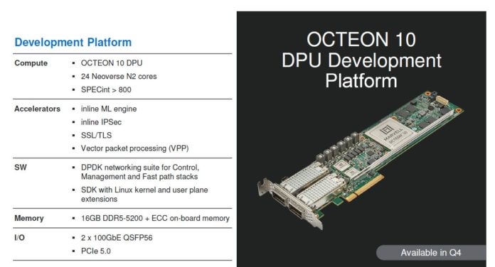
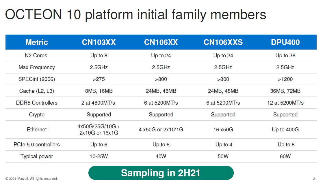
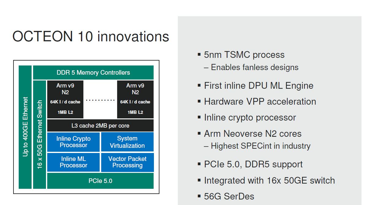
Marvell Octeon 10 400Gbps PCIe Gen5 DPUs Announced
TSMC 5nm
https://www.servethehome.com/marvell-octeon-10-400gbps-pcie-gen5-dpus-announced/
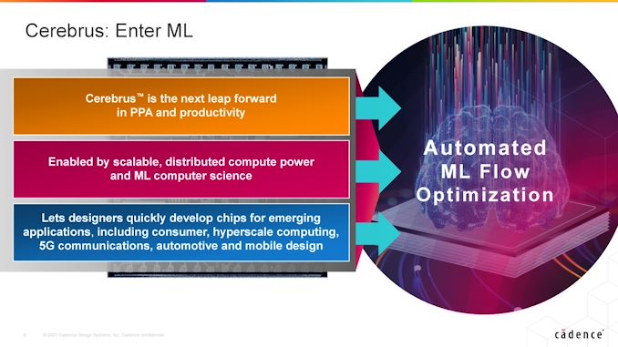
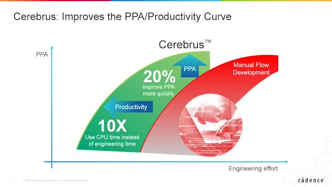
The design of most leading edge processors and ASICs rely on steps of optimization, with the three key optimization points being Performance, Power, and Area (and sometimes Cost). Once the architecture of a chip is planned, it comes down to designing the silicon of that chip for a given process node technology, however there are many different ways to lay the design out. Normally this can take a team of engineers several months, even with algorithmic tools and simulation to get a good result, however that role is gradually being taken over with Machine Learning methods.
Today’s announcement is from Cadence, one of the top EDA tool vendors, with the launch of their new Cerebrus technology. Integrated directly into the Cadence toolchain, Cerebrus can work at any level of the stack design, from high level definitions in System C down to standard cells, macros, RTL and signoff, and it allows an engineer to give it objects with defined specifications at any level and optimize for each. The automated floorplanning allows for the engineer to specify optimization points beyond regular PPA, such as wire length, wire delay, power grid distribution, IR drop, IO placement with respect to physical chip boundaries, and other parameters.
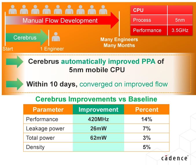
First up is a 5nm mobile CPU, which we believe to be part of Cadence’s partnership with Samsung Foundry. According to the information, the Cerebrus tool helped a single engineer in 10 days achieve a 3.5 GHz mobile CPU while also saving leakage power, total power, and improving transistor density. Compared to a predicted timeline using almost a dozen engineers over several months, it is predicted that Cerebrus improved the best hand tuned design for a +420 MHz frequency gain, saving 26 mW of leakage power and 62 mW of total power.
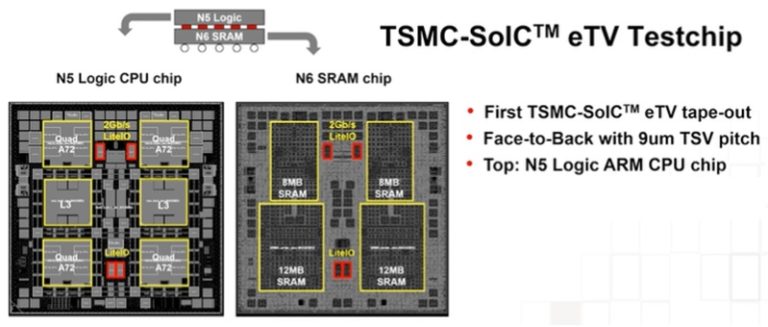
The configuration used was the vertical bonding of an (N5) CPU die with an (N6) SRAM die, in a face-to-back topology. (Indeed, a major CPU vendor has pre-announced plans for a vertical “last-level” SRAM cache die attached to a CPU using TSMC’s SoIC, to be available in 1Q2022.)

https://www.tomshardware.com/news/huawei-dyna-cloud-kirin-9006cThe Dyna Cloud L420 will reportedly use a brand-new in-house Arm SoC from Huawei called the Kirin 9006C. The SoC will contain 8 CPU cores, with the prime core(s) clocked at up to 3.1 GHz. In addition, it's also alleged that the SoC will feature a new GPU called the Kirin 9000C. Unlike PC-centric x86-64 processors from AMD and Intel, which are based on 7nm and 10nm process nodes, the Kirin 9006C uses a 5nm process like the latest mobile chips from Apple and Qualcomm.
TSMC (TWSE: 2330, NYSE: TSM) today introduced its N4X process technology, tailored for the demanding workloads of high performance computing (HPC) products. N4X is the first of TSMC’s HPC-focused technology offerings, representing ultimate performance and maximum clock frequencies in the 5-nanometer family.
https://pr.tsmc.com/english/news/2895These HPC features will enable N4X to offer a performance boost of up to 15% over N5, or up to 4% over the even faster N4P at 1.2 volt. N4X can achieve drive voltages beyond 1.2 volt and deliver additional performance. Customers can also draw on the common design rules of the N5 process to accelerate the development of their N4X products. TSMC expects N4X to enter risk production by the first half of 2023.
Year-over-year, second quarter revenue increased 43.5% while net income and diluted EPS both increased 76.4%. Compared to first quarter 2022, second quarter results represented an 8.8% increase in revenue and a 16.9% increase in net income.
Gross margin for the quarter was 59.1%, operating margin was 49.1%, and net profit margin was 44.4%.
https://investor.tsmc.com/english/e...2b7f088e2dee32e13a0bc/2Q22EarningsRelease.pdfIn the second quarter, shipments of 5-nanometer accounted for 21% of total wafer revenue; 7-nanometer accounted for 30%. Advanced technologies, defined as 7-nanometer and more advanced technologies, accounted for 51% of total wafer revenue