
muddymind
1st Folding then Sex
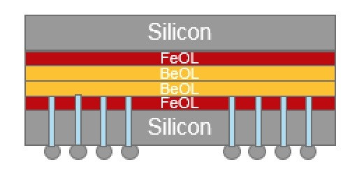
TSMC is close to adapt 3D stacked silicon wafers to complex silicon designs, such as graphics processors, using its new proprietary Wafer-on-Wafer (WoW) Advanced Packaging technology, which will be introduced with its 7 nm+ and 5 nm nodes. 3D stacked silicon fabrication is currently only implemented on "less complex" silicon designs, such as NAND flash, which don't run anywhere near as hot as complex designs ASIC designs, such as GPUs or CPUs. In its current form, TSMC achieved 2-layer stacks, in which two silicon layers that are "mirror images" of each other (for perfect alignment), sandwich bonding layers, through which pins for the upper layer pass through.
The bonding of the two layers is where the bulk of TSMC's innovations and "secret sauces" lie. For 3D NAND flash, multiple pancaked dies are wired out through their edges. You don't need as many pins to talk to a NAND flash die, as say a GPU die. For complex dies, designers have to pass thousands of pins through the "bottom layer," the connecting substrate, and eventually to the "top layer." The bottom layer hence is bumped out on both ends, one side interfacing with the package substrate for both dies, and the top side serving as a sort of substrate for the top die. This innovation is what TSMC calls "thru-silicon-vias" or TSVs.

WoW (wafer on wafer) is different from package-on-package or PoP (the way SoCs and DRAM packages are mated inside cellphones), in which two complete packages are wired out either concentrically on the PCB, or with pins on top of the SoC package interfacing with the DRAM package. The DRAM package needs fewer pins than the SoC, so it's more convenient having that on top. A WoW die sits inside a single package, and offers double the die area of a planar single-layer die. The bonding layers, the other key innovation of TSMC, not only helps mate the two packages, but also helps with thermal conductivity. There's division of labor between the two dies. The bottom layer has to bear the wiring of both dies, while the top layer has to dissipate heat from both dies. In this regard, the top layer gets some help from the fact that it has blank areas (where the bottom layer would normally have bumps to the package substrate).
fonte