
You are using an out of date browser. It may not display this or other websites correctly.
You should upgrade or use an alternative browser.
You should upgrade or use an alternative browser.
Gráfica Nvidia RTX 5000 Series "Blackwell"
- Autor do tópico Ansatsu
- Data Início
28GT/s num bus de 512bit são 1,8TB/s.
night_sign
Power Member
Desta vez irei dar o salto para Nvidia.
Vai ser mais um bom salto sem concorrência.
Vai ser mais um bom salto sem concorrência.
Miguel_Pereira
Power Member
28GT/s num bus de 512bit são 1,8TB/s.
Mas será que vai mesmo ter 512bit?
A 4090 tem 384bit, a velocidade da memoria vai aumentar substancialmente... Provavelmente não terá tanta largura.
Não faço ideia. Estava só a responder ao Ansatsu.
Rumores são rumores... Aquilo também fala de 28GT/s, mas a GDDR7 é suposto ser capaz de 32GT/s logo a abrir. Num bus de 384bits daria 1,5TB/s, o que me parece um salto geracional bastante bom e plausível.
Talvez os yields da GDDR7 não sejam assim tão bons.. Ou talvez precisem da BW extra para outras aplicações...
Ou talvez aquilo não passe de rumor...
NVIDIA Blackwell “GB203” GPU to feature 256-bit bus & GB205 with 192-bit, claims leaker
GeForce RTX 50: up to 512-bit memory bus, no 384-bit option?
https://videocardz.com/newz/nvidia-...-256-bit-bus-gb205-with-192-bit-claims-leaker
Nemesis11
Power Member
Versões para "compute":


Link para a Keynote. Dia 18, 20:00 de Lisboa:
Nvidia is on top of the world. They have supreme pricing power right now, despite hyperscaler silicon ramping. Everyone simply has to take what Nvidia is feeding them with a silver spoon. The number one example of this is with the H100, which has a gross margin exceeding 85%. The advantage in performance and TCO continues to hold true because the B100 curb stomps the MI300X, Gaudi 3, and internal hyperscaler chips (besides the Google TPU).
The GPU compute dies will remain on 4nm like Hopper, so the first time Nvidia is not opting for a node transition for their datacenter GPUs. This is quite noteworthy as Nvidia has shipped roughly ~800mm2+ for the V100, A100, and H100. Now instead of being able to shrink process nodes for a larger transistor budget, they have to double the amount of silicon. This is due to issues with TSMC’s original 3nm, N3B.
In addition, there will be up to 8 stacks of 8-hi HBM3E with up to 192GB capacity. Both SK Hynix and Micron are suppliers with the vast majority being SK Hynix. This is a change from SK Hynix being the sole supplier for the H100 ramp. Samsung continues to be the laggard despite their announcements of developing “the world’s fastest” HBM3E. Samsung loves press releases, but they are currently facing major challenges in qualifications.
The B100 package is much larger, and as such it will be the first major high volume product utilizing CoWoS-L. CoWoS-L is an organic RDL substrate with passive silicon bridges.
The first version of Blackwell, codename Umbriel, is for time to market, it keeps PCIe Gen 5, 400G networking, etc. In fact, the B100 air-cooled 700W can even slide into existing servers that accept the H100 and H200 baseboards with nearly no modifications.
The B200 will follow shortly after, with a higher power limit of 1,000W. This version requires a redesign of servers. Based on checks from our newest analyst in Taiwan, Chaolien, the 1,000W version can still be air-cooled, which will come as a surprise to many.
For the standard GPU only product, Miranda comes after Umbriel. Miranda has PCIe Gen 6 and up to 800G networking. It has up to 192GB on the roadmap. However, Nvidia has already bought up all the supply of 36GB HBM which SK Hynix and Micron are ramping early next year. This means that there can be a refresh that actually goes up to 288GB per GPU.
https://www.semianalysis.com/p/nvidia-b100-b200-gb200-cogs-pricingThe product everyone in the supply chain is buzzing for is the Oberon GB200 platform.
Link para a Keynote. Dia 18, 20:00 de Lisboa:
NVIDIA GTC 2024 Keynote Coverage New CPUs GPUs and More
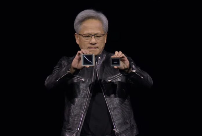
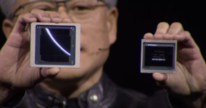
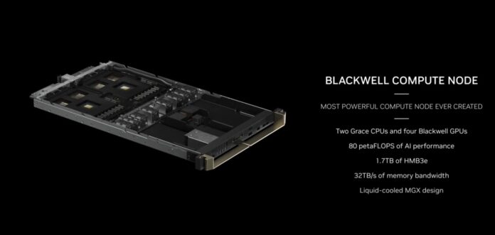
This is Blackwell and Hopper next to one another.
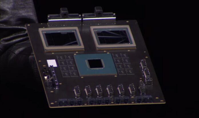
Here is the NVIDIA Grace Blackwell with two Blackwell GPUs, and one Grace CPU with memory for each. There is NVLink at the top of the board and PCIe at the bottom of the board.
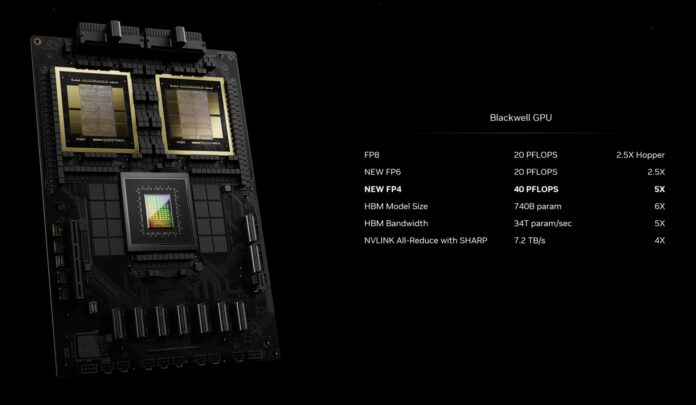
FP4 and FP6 add a ton of performance over Hopper.
Here is the overview of the NVIDIA Blackwell Compute Node.
https://www.servethehome.com/nvidia-gtc-2024-keynote-coverage-new-cpus-gpus-and-more/
Nvidia turns up the AI heat with 1,200W Blackwell GPUs
Of course, the devil is in the details, and getting this performance will depend heavily on a number of factors. While Nvidia claims the new chip will do 20 petaFLOPS, that's only when using its new 4-bit floating point data type and opting for liquid-cooled servers. Looking at gen-on-gen FP8 performance, the chip is only about 2.5x faster than the H100.
At the time of writing, Blackwell encompasses three parts: the B100, B200, and Grace-Blackwell Superchip (GB200). Presumably there will be other Blackwell GPUs at some point – like the previously teased B40, which use a different die, or rather dies – but for now the three chips share the same silicon.
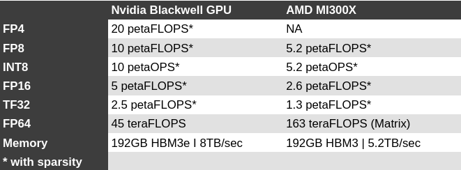
https://www.theregister.com/2024/03/18/nvidia_turns_up_the_ai/In terms of performance, the MI300X promised a 30 percent performance advantage in FP8 floating point calculations and a nearly 2.5x lead in HPC-centric double precision workloads compared to Nvidia's H100.
Comparing the 750W MI300X against the 700W B100, Nvidia's chip is 2.67x faster in sparse performance. And while both chips now pack 192GB of high bandwidth memory, the Blackwell part's memory is 2.8TB/sec faster.
Memory bandwidth has already proven to be a major indicator of AI performance, particularly when it comes to inferencing. Nvidia's H200 is essentially a bandwidth boosted H100. Yet, despite pushing the same FLOPS as the H100, Nvidia claims it's twice as fast in models like Meta's Llama 2 70B.
While Nvidia has a clear lead at lower precision, it may have come at the expense of double precision performance – an area where AMD has excelled in recent years, winning multiple high-profile supercomputer awards.
According to Nvidia, the Blackwell GPU is capable of delivering 45 teraFLOPS of FP64 tensor core performance. That's a bit of a regression from the 67 teraFLOPS of FP64 Matrix performance delivered by the H100, and puts it at a disadvantage against AMD's MI300X at either 81.7 teraFLOPS FP64 vector or 163 teraFLOPS FP64 matrix.
fire_rainbow
Power Member
NVIDIA Audio2Face uses AI to generate lip synching and facial animation, showcased in two games
https://www.tweaktown.com/news/9696...l-animation-showcased-in-two-games/index.html
https://www.tweaktown.com/news/9696...l-animation-showcased-in-two-games/index.html
O que mais achei interessante que são dois dies com interconnect.
Será que as versões desktop poderão ter isso? um die com 128 bits e dai surge placas de 128 (1 dies), 256(2 dies), 384 (3 dies).
ou 2 dies maiores com 256 bits, mas ai terá um gap enorme, a não ser que apareça um GPU intermediário com 192 bits x 2 (384 bits).
Será que as versões desktop poderão ter isso? um die com 128 bits e dai surge placas de 128 (1 dies), 256(2 dies), 384 (3 dies).
ou 2 dies maiores com 256 bits, mas ai terá um gap enorme, a não ser que apareça um GPU intermediário com 192 bits x 2 (384 bits).
Poder podem, mas não estou a ver a Nvidia a gastar tempo e dinheiro com isso, até porque aparentemente a "limitação" na produção dos chips multi die, com esta complexidade, é precisamente a "montagem" dos mesmos.
Embora não tenham feito, acho eu, referência a isso é quase certo que é o "CoWoS" da TSMC, que apesar do sucessivo investimento na expansão da capacidade continua a estar aquém das necessidades, quer da TSMC quer de outras OSAT.
Embora não tenham feito, acho eu, referência a isso é quase certo que é o "CoWoS" da TSMC, que apesar do sucessivo investimento na expansão da capacidade continua a estar aquém das necessidades, quer da TSMC quer de outras OSAT.
TSMC Reportedly Doubles CoWoS Capacity while Amkor, ASE also Enter Advanced Packaging for AI
https://www.trendforce.com/news/202...kor-ase-also-enter-advanced-packaging-for-ai/The surge in demand for advanced packaging is being primarily propelled by artificial intelligence (AI) chips. According to industry sources cited by CNA, TSMC’s CoWoS production capacity is set to double this year, yet demand continues to outstrip supply. In response, NVIDIA has enlisted the help of packaging and testing facilities to augment its advanced packaging capabilities.
In addition, to address the imbalance between supply and demand for advanced packaging due to AI, semiconductor backend specialty assembly and testing (OSAT) companies such as ASE Technology Holding (ASE), Powertech Technology, and KYEC have expanded their capital expenditures this year to enhance their advanced packaging capabilities, aligning with the needs of their customers.
AI and high-performance computing (HPC) chips are driving the demand for CoWoS advanced packaging. As per sources interviewed by CNA, from July to the end of last year, TSMC actively adjusted its CoWoS advanced packaging production capacity, gradually expanding and stabilizing mass production.
The source further indicates that in December of last year, TSMC’s CoWoS monthly production capacity increased to 14,000 to 15,000. It is estimated that by the fourth quarter of this year, TSMC’s CoWoS monthly production capacity will significantly expand to 33,000 to 35,000.
TSMC Boosts Investment in Advanced Packaging with NTD 500 Billion Plan to Build Six Plants in Chiayi Science Park
The Executive Yuan and TSMC have reportedly reached a consensus on the investment project for the new advanced packaging plant at the TSMC Science Park in Chiayi. According to a report from Economic Daily News, six new plant sites will be allocated to TSMC in the Science Park, two more than originally anticipated, with a total investment exceeding NTD 500 billion. The expansion is expected to increase CoWoS advanced packaging capacity and to be announced to the public in early April.
https://www.trendforce.com/news/202...n-to-build-six-plants-in-chiayi-science-park/TSMC’s extensive expansion is primarily driven by the high demand for advanced packaging. For instance, in the case of the NVIDIA H100, after integrating components via CoWoS, each wafer yields approximately 28 chips. However, for the upcoming B100, with increased volume and integration, the yield per wafer drops to just 16 chips.
PipocaGorda
Power Member
Aos preços que vou comprar a próxima placa, vem de certeza uma AMD. Com o AI a Nvidia vai deixar de se preocupar com a relação de preço performace e o DlSS vai deixar de ser um diferenciador. Espero é que as Nvidias sejam tão boas que os preços das AMD venham por aí abaixo 
Raptor
OC Legend
A grande vantagem disso é fazerem o mesmo que fizeram com o PCIe 4.0 em modelos da gama RTX 4060, usar interface mais rápida, mas reduzir o número de pistas utilizadas (ex. PCIe 5.0 x8). É uma bela forma de reduzir os custos de produção, e aumentarem os lucros. A Nvidia tem-se tornado especialista nesta última matéria.Podes ir para B650E também.
Não acho que PCIE 5.0 faça diferença, mesmo hoje entre 3.0 e 4.0 @ x16 quase não há perda de performance a não ser que metam PCIE 4x e 8x nas gráficas low/mid.

Ansatsu
Power Member
Teoricamente a 5070 tem de ser mais potente que a 3080 Ti, se vai valer a pena o upgrade já será uma historia bem diferente.O que esperar da 5070 vs 3080ti? Será uma diferença de performance considerável e que vai valer o upgrade?
Vai depender das features exclusivas da serie 5000 e do quao potente o Gpu sair.
Ainda sai este ano a série 5000?Teoricamente a 5070 tem de ser mais potente que a 3080 Ti, se vai valer a pena o upgrade já será uma historia bem diferente.
Vai depender das features exclusivas da serie 5000 e do quao potente o Gpu sair.