Processador Intel Sandy Bridge - 2100 / 2400 / 2500(K) / 2600(K) / 2700k - Socket 1155/2011

Nemesis11

Power Member
snb2496035366.jpg


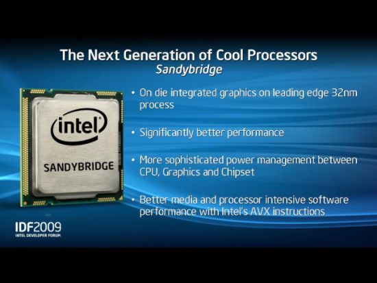
While we can not reveal to you some details of the architecture in the heart of Sandy Bridge, a few remain unknown. First, the Socket. According to the noises heard in corridors at a manufacturer of motherboard, the CPU should resume Socket 1156 of Clarkdale (generation "Westmere" above) but require a new chipset. Then, the performance of the integrated circuit graphics are all subject to speculation. We already know that the IGP Sandy Bridge will always be based on GMA and not on any variation of Larabee. With a frequency of approximately 1.2 GHz, this heart intended to be compatible with DirectX 11, should not be ridiculous but be a lightning war. Finally, the number of PCI Express link is still unknown. According to the first draft of the datasheet, this heart contain 20 lines PCI Express 2.0 (16x + 4x), but the information could not be confirmed ...

http://www.canardpc.com/news-37333-...en_photo_le_futur_sandy_bridge_d___intel.html

Apesar de ainda ser só um die shot é interessante ver integrado no cpu:
- Northbridge
- Gpu, baseado no GMA
- Links Pci-Express
- Ring bus para aceder à L3, que não é só acedido pelos cpu, mas também pelo gpu.
- AES e AVX instructions.

Este deve ser a versão mainstream.Devem existir várias variações para diferentes mercados.
 
Bem pensado a ligação do GPU à L3...sempre será mais rápido que aceder à RAM. Agora falta saber quais as implicações na performance do CPU ao partilhar a L3 com o GPU...

Imaginemos que estamos a jogar um jogo já antigo (tipo Halo2) e aplicamos AA, presumo que o GPU irá usar a L3 para ajudar no AA já que é mais rápida (não sei se estou correcto mas penso que a velocidade da memorias seja importante, isto pelo que vi no GPU da X360...) e a RAM para o resto (texturas e afins) e o CPU? Fica apenas com a L2? que nem sequer é partilhada? Não sei...

Não seria preferível algo deste género: (?)

EDIT: A não ser que a Intel se tenha lembrado disto... (LOL), e tenha feito:
Os Cores conseguem aceder à cache L2 uns dos outros, assim funcionaria como uma shared.
 

Anexos

  • Sem título.jpg
    Sem título.jpg
    19,5 KB · Visualizações: 264
Última edição:
Mas, porque partilhar a cache L2, se basta a graaande L3, mesmo sendo mais lenta... Anyway... Estou feliz por ver o substituto do meu Q6600 ^_^
 
Mas, porque partilhar a cache L2, se basta a graaande L3, mesmo sendo mais lenta... Anyway... Estou feliz por ver o substituto do meu Q6600 ^_^

O IGP só poderia estar ligado à L3. É por esta parte do chamado "uncore" que também passa o tráfego do controlador de memória.

Quanto ao IGP se basear na "tecnologia" GMA, isso não quer dizer nada.
Há GMA's com tecnologia da Real3D (os mais antigos), outros desenhados in-house com alguma IP licenciada de terceiros, e outros ainda licenciados directamente à ImTech (GMA 500, a.k.a. PowerVR SGX 5xx).
 
sempre se volta ao dual channel

pouca cache...

Não sei se viu bem a figura, mas ali refere que é uma versão mainstream, nem sequer é o Sandy high end.

Bem pensado a ligação do GPU à L3...sempre será mais rápido que aceder à RAM. Agora falta saber quais as implicações na performance do CPU ao partilhar a L3 com o GPU...

Imaginemos que estamos a jogar um jogo já antigo (tipo Halo2) e aplicamos AA, presumo que o GPU irá usar a L3 para ajudar no AA já que é mais rápida (não sei se estou correcto mas penso que a velocidade da memorias seja importante, isto pelo que vi no GPU da X360...) e a RAM para o resto (texturas e afins) e o CPU? Fica apenas com a L2? que nem sequer é partilhada? Não sei...

Não seria preferível algo deste género: (?)

EDIT: A não ser que a Intel se tenha lembrado disto... (LOL), e tenha feito:
Os Cores conseguem aceder à cache L2 uns dos outros, assim funcionaria como uma shared.

Não faz muito sentido para um produto mainstream. Ao leres a notícia reparas que o GPU será ainda baseado nos antigos GMA, e não no Larrabee. O que estás a falar seria algo do tipo eDRAM, mas isso nem sequer é utilizado em GPUs desktops, portanto até isso ser viável num produto mainstream terão que passar muitos mais anos. Repara que o próprio Clarkdale era para vir também com o CPU em 45nm, mas no fim virá a 32nm, apesar do GPU ser ainda de 45nm.

Em relação a ligação com a Cache L3 não passa disso mesmo... uma ligação. A não ser que o GPU seja suficiente "inteligente" em buscar e encontrar dados partilhados com outros respeitantes ao CPU em si.

Eles aqui decidiram integrar o GPU no CPU e não em separado, mesmo em 32nm daí o TDP ser bastante elevado para um produto de entrada de gama. Aquelas velocidades de relógio é que são mínimo "mágicos". ;)
 
Não podes ver o TDP apenas por ser CPU.

Quanto que é o TDP actual de um quad + northbridge? pois.

Alem disso, não está previsto sair na geração nehalem um quad com IGP, ficando apenas pelos dual core.

E depois ver se aquelas frequências do IGP poderão fazer algum... milagre. É quase o dobro do clock de qualquer GPU discrete actual (claro que o clock não é tudo)

o actual GMA x4500 tem 800 mhz, portanto esse a partida tem mais 50% clockspeed. Juntando mais shaders, dx11, ligação directa pela L3, etc, quem sabe apareça ai algo com a partida 8x mais potencia que o actual x4500. Falta faltar algo que a Intel não tem de bom, drivers de jeito!

Não estamos obviamente a falar de uma RV770 onboard, mas talvez encare coisas como 3600/4500
 
Última edição:
Para mim, podem tirar o IGP... não planeio ter gráficas onboard... e o freespace usavam pra meter mais cache L3 :D

EDIT: A não ser que a Intel se tenha lembrado disto... (LOL), e tenha feito:
Os Cores conseguem aceder à cache L2 uns dos outros, assim funcionaria como uma shared.
Não percebo o porque de tb ter a cache L2 partilhada... para isso, porque raio é que existia cache L3?? o IGP deve usar apenas memória DDR3/4 não parte da cache L3 (digo eu).
 
Última edição:
Não sei se viu bem a figura, mas ali refere que é uma versão mainstream, nem sequer é o Sandy high end.


Não faz muito sentido para um produto mainstream. Ao leres a notícia reparas que o GPU será ainda baseado nos antigos GMA, e não no Larrabee. O que estás a falar seria algo do tipo eDRAM, mas isso nem sequer é utilizado em GPUs desktops, portanto até isso ser viável num produto mainstream terão que passar muitos mais anos. Repara que o próprio Clarkdale era para vir também com o CPU em 45nm, mas no fim virá a 32nm, apesar do GPU ser ainda de 45nm.

Em relação a ligação com a Cache L3 não passa disso mesmo... uma ligação. A não ser que o GPU seja suficiente "inteligente" em buscar e encontrar dados partilhados com outros respeitantes ao CPU em si.

Eles aqui decidiram integrar o GPU no CPU e não em separado, mesmo em 32nm daí o TDP ser bastante elevado para um produto de entrada de gama. Aquelas velocidades de relógio é que são mínimo "mágicos". ;)
Exacto seria tipo a eDRAM, sempre era capaz de dar uma "ajuda" ao GPU...visto ainda ser uma GMA.

Para mim, podem tirar o IGP... não planeio ter gráficas onboard... e o freespace usavam pra meter mais cache L3 :D


Não percebo o porque de tb ter a cache L2 partilhada... para isso, porque raio é que existia cache L3?? o IGP deve usar apenas memória DDR3/4 não parte da cache L3 (digo eu).

Se não usar a L3 não faz sentido a L2 parilhada, disse o que disse porque me dava a entender que ele poderia usar a L3 como um eDRAM, e penso que nesse caso em aplicações 3D mais pesadas o GPU ia prejudicar a performance do CPU. Mas se virmos bem, vai acabar sempre por prejudicar... ele vai usar o IMC parar aceder à RAM, logo à partida vai "comer" largura de banda.

Isto num dual-core faz mais sentido.
 
Para mim, podem tirar o IGP... não planeio ter gráficas onboard... e o freespace usavam pra meter mais cache L3 :D


Não percebo o porque de tb ter a cache L2 partilhada... para isso, porque raio é que existia cache L3?? o IGP deve usar apenas memória DDR3/4 não parte da cache L3 (digo eu).

É obvio que vai existir versão sem GPU. Não me admira que apareça uns octo-core tb :004:

Este CPU é voltado para sistema non-gamming.

A vantágem de integrar o IGP é alem de potencial melhor performance, é diminuir o TDP do sistema.

85w para um quad core + igp + northbridge é muito bom. 90w é o TDP de um q9xxx, fora o consumo do G45

Por estar ligado à L3, tens um bus de altíssima velocidade
 
Última edição:
O facto de estar ligado a L3 para comunicar sempre ajuda, mas como solução integrada, vai continuar a usar a memória do sistema para guardar dados. Assim sendo vai continuar a ocupar bus de memória, e vai adicionar como sempre alguma latência extra.

cachemem1066.jpg


Ao contrário do i7 Bloomfield, não esquecer que de acordo com a informação do primeiro post, o bus de memória será dual-channel.

Se bem que quando se altera a velocidade do CPU, a svelocidades de acesso as caches L1, L2 e L3 acabam por subir também, já que estão todos integrados no CPU. Aquelas velocidades de relógio até 3.8GHz devem servir para compensar a latência extra que a L3 vai sofrer por causa da conexão com o GPU.

E não estou convencido com aquelas velocidades de relógio, sobretudo quando estamos a falar do modelo mainstream... a não ser haja algum alteração substâncial no Sandy Bridge para conseguir atingir tais velocidades de relógio.

EDIT: Olhando melhor aquele T depois do 3.8GHz até pode ser a velocidade em Turbo Mode.

EDIT2: Também está referido no próprio link para a fonte:

Côté fréquence, il faudra encore attendre quelques steppings pour connaitre les limites de ce cœur, mais les premières estimations sont comprises entre 2.8 et 3.4 GHz, avec un mode Turbo compris entre 3.8 et 4 GHz. N’oubliez pas que ce processeur ne sera pas le haut de gamme de l’époque. D’autres versions, dotés de 2 et 8 cœurs sont également prévues (avec respectivement 4 et 16 Mo de cache L3) mais ne sont pas encore disponible à l’état de prototype.
 
Última edição:
Sandy Bridge 32nm has on die integrated graphics
According to IDF slides, Sandy Bridge might be the first Intel CPU to get fully integrated graphics. Intel and Didi in his presentation hinted that in late 2010 you can expect „on die integrated graphics on leading edge 32nm process“.

Intel also promises better performance, and this was something that they executed well in the last few years. This chip might be even better for mobile as it should come with more sophisticated power management between chipset CPU and graphics. Didi also promised better graphics for it.

Intel also talked about its new AVX instructions that should enable better media and processor intensive software performance.

The question remains if Sandy Bridge, at least in its mobile version, has a native 32nm graphics core that will be fully integrated in the CPU, but this sounds quite aggressive and with live samples running on stage, it looks that Intel has already scored the next winner.

intelsandyslide.jpg
 
Intel Sandy Bridge 32nm comes in Q1 2011


Tick - Tock got broken Intel played their tick - tock strategy for a few years and it looks like they won’t be able to launch this part in Q4 2010 and make it in year 2010. We are sure Intel will tell us that the production starts in Q4 2010 but the availability will happen in Q1 2011. Sandy Bridge is a new architecture, a step after Nehalem / Lynnfield / Clarkdale generation and it should bring more integration between graphics and CPU and generally make things faster. It's in 32nm and you can expect a new graphics core as well as Turbo overclocking and continuation of the quite useless hyperthreading strategy. We can only hope that Intel will hire some people from Switzerland who are capable of fixing the broken tick - tock but kudos to Intel for being on time since summer 2006.

Dados Wiki:


  • A0 Stepping
  • 2.8 GHz to 3.4 GHz clock speed with Turbo Boost Technology disabled.
  • 3 GHz to 3.8 GHz clock speed with Turbo Boost Technology enabled.
  • Processing cores will feature Hyper-Threading Technology that is also present in Intel Nehalem-based processors, as well as Intel Pentium 4 processors.
  • 4 cores by default.
  • Approximate 225 mm² die size by default.
  • Without SSE: 8 DP GFLOPS/core (2 DP FP/clock), 32-64 DP GFLOPS per processor.
  • With SSE: 32 DP GFLOPS/core (8 DP FP/clock), 128-256 DP GFLOPS/processor.
  • 256 KB L2 cache/core, (9 clocks).
  • 8 MB shared L3 cache (25 clocks). This L3 cache will also be shared with the integrated graphic core.
  • 64 bytes cache line width.
  • Integrated graphics core running at 1 GHz to 1.4 GHz.
  • Integrated Memory Controller with maximum 25.6 GB/s bandwidth, supports DDR3-1600 dual channel RAM.
  • 256 bit/cycle Ring bus bandwidth. The ring bus connects the cores.
  • Maximum Thermal Design Power (TDP) of just 85W by default.
  • Release date is expected at Q1 2011.
According to some PC Watch articles:[6][7]

  • Sandy Bridge will be an evolutionary step from Core 2.
  • Sandy Bridge will focus on power efficiency.
  • Performance will be increased without a core size increase (similar to the Netburst to Core transition).
  • The CPU core is scalable.
  • Due to the small 32 nm process, the floating point unit is small compared to the rest of the core.
  • Dynamic Turbo allows the CPU power to exceed the TDP value when the rest of the platform is relatively cool. The frequency gain can be up to 37% for one minute, and over 20% in most cases.
  • Nehalem may stay at the server platform while Sandy Bridge is released for the mobile segments, which would split the markets into two CPU lines.
  • Sandy Bridge's CPU and GPU are likely to be on one die (unlike the two-die approach of Nehalem).
  • Because of the high-performing CPU and off-chip components, it may be necessary to improve bus interconnects. The internal bus is to be improved.
  • The Sandy Bridge microarchitecture is also said to focus on the connections of the processor core.
  • If the transition to 22 nm is difficult, then Sandy Bridge may go over three generations (Sandy Bridge, Ivy Bridge, and another Bridge) as opposed to two with Nehalem and Core 2.
The mobile Sandy Bridge version is expected to be released at the same time as the microarchitecture.[8] The platform chipset's northbridge is referred to as the 'Sandy Bridge System Agent' rather than 'MCH'.[9]
Intel has said that Sandy Bridge will have new instructions called Advanced Vector Extensions (AVX).[10] These instructions are an advanced form of SSE. The data path is widened from 128 bits to 256 bits, the two-operand instruction limit is increased to three operands, and advanced data rearrangement functions are included. AVX is suited for floating-point-intensive applications.[11] Features of AVX include mask loads, data permutes, increased register efficiency and use of parallel loads, as well as smaller code size. The improvements of AVX will allow it to deliver up to double the peak FLOPS compared to before. Sandy Bridge will also have a new extensible VEX opcode prefix.[12]
EDIT: Se não me engano Sandy Bridge sai ao mesmo tempo dos AMD 32nm Bulldozer... Vai ser um Q1/2011 muito, muito fixe :D

Filme de um Sandybridge a trabalhar no IDF09.
 
Última edição:
A tirar disso aparentemente vai sair primeiro para portáteis (não com este TDP, obviamente).

E depois é esperar pelas gerações sem IGP (quads mais eficientes e six-core)
 
Sandy Bridge CPU to have up to 2 GPUs

Monolithic on-die


We were quite shocked to learn that Intel might be the first company to ever launch two GPUs on the same die. Not only does it look like Intel might be the first with monolithically integrated with the CPU and have Fusion before AMD, bit it might be the first “graphics” company to ever launch two GPUs on the same die.

According to Intel’s plans that were revealed to partners and industry insiders Sandy Bridge, brand new 32nm architecture will have one to two graphics cores on a monolithic die.

Intel will also let you connect discrete graphics via PCIe 16X and even SLI / Crossfire should be possible with 2x 8X PCIe slots. This is likely to happen on desktop boards rather than notebook.

At this time we are not aware that Nvidia and ATI will launch their dual GPU solutions on a single chip, but if you look a high-end card, for example a Fermi, it card has 512 shader cores and if you cut it in half you get a mainstream card. With this in mind, ATI and Nvidia practically make high-end chips out of four low end GPUs.
 
Com isto já sei quando devo actualizar o meu computador, de raiz :D

Anyway de que vai servir aquele GPU integrado ? Ou dois, performance equivalente a que ?
 
Com isto já sei quando devo actualizar o meu computador, de raiz :D

Anyway de que vai servir aquele GPU integrado ? Ou dois, performance equivalente a que ?

Nem com dois GPU's devem conseguir sair do segmento low-end... As gráficas da intel são fracas e PONTO FINAL! Portanto isto de ter 2 GPU's só se for para suportar mais outputs porque de resto é uma parvoíce... É como as gráficas low-end com 2GB de RAM :D viva o markting :rolleyes:
 
Intel to Release Sandy Bridge Processors, New Infrastructure in Q1 2011 – Source


Intel Corp. plans to release its next-generation microprocessors based on the code-named Sandy Bridge micro-architecture in Q1 2011, sources familiar with Intel Corp.’s plans told X-bit labs. The initial processors based on the new micro-architecture will not aim at the high-end market, but will still not be compatible with current mainstream infrastructure and will require new sockets and chipsets.
The first Intel Sandy Bridge chips will feature two or four cores with Turbo Boost and Hyper-Threading technology as well as integrated graphics processor that will actually be on the same die as the x86 cores, according to previous reports. The chips will address mainstream market segments currently served by Intel Core i7, Core i5 and Core i3 processors, hence, there will be a lot of different models with 65W (dual-core, quad-core)or 95W (quad-core) thermal design power. The new processors will use LGA1155 form-factor and will be compatible with platforms based on the Intel 6-series chipsets code-named Cougar Point. It is noteworthy that while the new 6-series mainstream chipsets support Serial ATA-600 and some other innovations, the USB 3.0 does not seem to be a capability of the core-logic.
Some reports claim that six-core and eight-core Sandy Bridge-based designs will become available in Q2 2011 or later, hence, Intel is taking the same strategy as with Westmere micro-architecture and plans to initiate production of less complex processors first with higher-end models following later.
The key feature of Sandy Bridge Intel AVX (Advanced Vector Extensions) which, when used by software programmers, will increase performance in floating point, media, and processor intensive software, according to the Intel. Key features of Intel AVX include wider vectors, increasing from 128 bit to 256 bit wide, resulting in up to 2x peak FLOPs output. Enhanced data rearrangement, resulting in allowing data to be pulled more efficiently, and three operand, non-destructive syntax for a range of benefits. Intel AVX can also increase energy efficiency beyond the increases brought by the micro-architectural innovations, and is backwards compatible to existing Intel processors.
Intel did not comment on the news-story.
 
De certa forma até são boas notícias para a AMD que vê o seu fusion lançado +\- na mesma altura que a intel lança o substituto do clarckdale e ambas as plataformas irão precisar de novos sockets e com a vantagem de ter tdp's bem mais baixos (se bem que ainda estou muito céptico relativamente aos tdp's prometidos pela AMD).
 
Back
Topo