
You are using an out of date browser. It may not display this or other websites correctly.
You should upgrade or use an alternative browser.
You should upgrade or use an alternative browser.
Globalfoundries/TSMC 7nm (2018)
- Autor do tópico Dark Kaeser
- Data Início
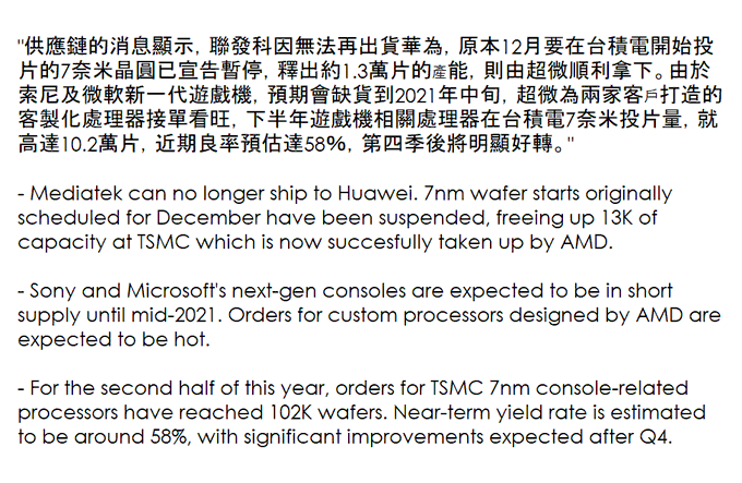
E entretanto confirma-se:
A Digitimes há uns tempos tinha dito que as encomendas da HiSilicon tinham sido divididas pela Mediatek e AMD.
Taiwan Semiconductor Manufacturing Co. on Thursday confirmed it has suspended processing new orders from key customer Huawei Technologies to comply with U.S. export regulations,
https://asia.nikkei.com/Spotlight/H...s-to-halt-chip-supplies-to-Huawei-in-2-months"We are complying fully with the new [U.S.] regulations. We did not take any new orders [from Huawei] since May 15," TSMC Chairman Mark Liu told an investors conference, confirming an earlier report by the Nikkei Asian Review. "Although the regulation just finished its public comment period, the BIS [Bureau of Industry and Security] did not make a final ruling change. Under this circumstance, we do not plan to ship wafers [to Huawei] after Sept. 14."
A Digitimes há uns tempos tinha dito que as encomendas da HiSilicon tinham sido divididas pela Mediatek e AMD.
Nemesis11
Power Member
Mas atenção a esta parte do artigo:
A TSMC pode pedir uma licença ao Governos dos Estados Unidos, para ter uma excepção e assim poder fabricar chips para a Huawei.
Além disso, este processo está a decorrer com a legislação actual. Como isto só se aplica a partir de 14 de Setembro, se alguma coisa se alterar até lá, isto tudo pode mudar.
Outras coisas que se deve ter em conta:
A curto prazo, os USA podem ganhar a guerra e conseguirem o que querem. A curto prazo, a China poderá ter muitas dificuldades nesta área, mas a médio/longo prazo, acho que só vai fazer com que a China fique mais convencida que não podem ficar dependentes de ninguém externo e apostar e investir muito no desenvolvimento interno de empresas ligadas a hardware e software. Em algumas áreas já se vêm nascer iniciativas interessantes nesta área.
Normalmente, nestas guerras económicas, todos os países envolvidos saem a perder, de uma forma ou de outra.
Under the tightened export control rule, non-U.S. chip companies must apply for licenses to use American technology and tools to supply to Huawei, the biggest Chinese tech company. TSMC and other chipmakers were not allowed to process new orders from Huawei or its chip design arm HiSilicon after May 15 without a license and must ship any orders already in the pipeline before Sept. 14.
Liu did not say whether TSMC plans to apply for licenses to ship to Huawei. A TSMC spokesperson said the chairman's comment is based on current rules, and it is not clear whether there will be any further regulation changes from the U.S. government, given that the comment period just ended a few days ago.
A TSMC pode pedir uma licença ao Governos dos Estados Unidos, para ter uma excepção e assim poder fabricar chips para a Huawei.
Além disso, este processo está a decorrer com a legislação actual. Como isto só se aplica a partir de 14 de Setembro, se alguma coisa se alterar até lá, isto tudo pode mudar.
Outras coisas que se deve ter em conta:
- As eleições nos USA são a 3 de Novembro e depois dessa data, as coisas podem mudar para um lado e para o outro, seja qual for a pessoa que seja eleita.
- Por mera curiosidade, a TSMC é uma empresa sediada em Taiwan e a maior empresa de fornecimento de maquinaria para produção de semicondutores, a ASML, está sediada na Holanda. As duas têm bases nos USA, especialmente a ASML, mas não deixa de mostrar a influencia que os USA têm.
A curto prazo, os USA podem ganhar a guerra e conseguirem o que querem. A curto prazo, a China poderá ter muitas dificuldades nesta área, mas a médio/longo prazo, acho que só vai fazer com que a China fique mais convencida que não podem ficar dependentes de ninguém externo e apostar e investir muito no desenvolvimento interno de empresas ligadas a hardware e software. Em algumas áreas já se vêm nascer iniciativas interessantes nesta área.
Normalmente, nestas guerras económicas, todos os países envolvidos saem a perder, de uma forma ou de outra.
Sim, mas as declarações surgem após a questão sobre se a HiSilicon colocou mais alguma encomenda após 15 de Maio, que era a data limite da tal resolução do EUA.
A própria Digitimes já tinha reportado que face a essa resolução a HiSilicon e a TSMC tinham tentado junto dos restantes clientes a 7nm antecipar as encomendas para poder satisfazer o fabrico dos chips até Setembro.
A própria Digitimes já tinha reportado que face a essa resolução a HiSilicon e a TSMC tinham tentado junto dos restantes clientes a 7nm antecipar as encomendas para poder satisfazer o fabrico dos chips até Setembro.
Querem lá ver
Aparentemente o destinatário será o próprio governo chinês.
https://www.techpowerup.com/270903/...peng-cpu-reportedly-beats-intel-core-i9-9900kThe specific chip used in this upcoming computer is the Kunpeng 920 3211K CPU which features 24 cores clocked at 2.6 GHz paired with 8 GB DDR4 memory, 512 GB Samsung SSD, and an AMD Radeon RX 520 GPU.
Aparentemente o destinatário será o próprio governo chinês.
Nemesis11
Power Member
Dizer que um processador de 24 cores fabricados a 7nm é um pouco mais rápido em multithread que um processador de 8 cores num processo de fabrico 1 geração atrás, não é propriamente o maior feito do mundo. Ok, o 9900K tem um clock muito elevado, mas provavelmente os Atoms para servidores, com 16 cores, também são capazes de bater o 9900K em alguns benchmarks. Aí também está o segundo problema. Não dizem que benchmarks usaram.
Também espero que produzam boas quantidades até a TSMC fechar a torneira. Não se sabe se e quando a TSMC vai voltar a produzir para a Huawei.
Por fim, algo um bocado estranho no artigo original:
Supostamente, só leva as Radeons 520 e não funciona com outras placas gráficas. Estranho, porque se vai usar Linux, não deveria ter problemas com outras gráficas.
Também espero que produzam boas quantidades até a TSMC fechar a torneira. Não se sabe se e quando a TSMC vai voltar a produzir para a Huawei.
Por fim, algo um bocado estranho no artigo original:
In terms of expansion, this desktop does not support other types of graphics cards
Supostamente, só leva as Radeons 520 e não funciona com outras placas gráficas. Estranho, porque se vai usar Linux, não deveria ter problemas com outras gráficas.
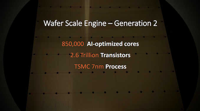
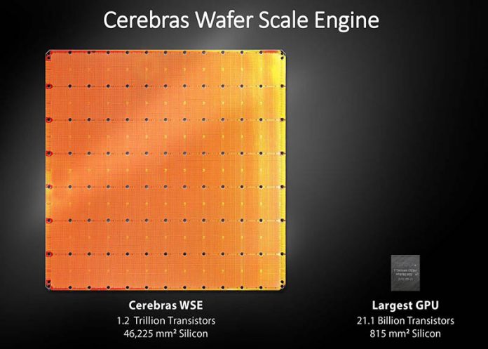
Para comparação, esta é a 1ª
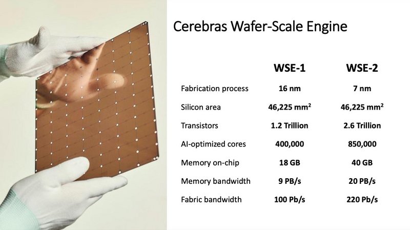
The chip itself was rectangular, but it was cut from a single wafer, and contained 400,000 cores, 1.2 trillion transistors, 46225 mm2 of silicon, and was built on TSMC’s 16 nm process.


0 ou 1 
Na realidade isso foi debatido no ano passado.
Mas tem outras coisas curiosas
https://www.servethehome.com/cerebras-wafer-scale-engine-ai-chip-is-largest-ever/
Em relação ao sistema propriamente dito mostraram em Dezembro passado ns SC'19
https://www.servethehome.com/cerebras-cs-1-wafer-scale-ai-system-at-sc19/
Só para se ter a noção
Só mesmo naquela da curiosidade, o CEO da Cerebras é o Andrew Feldman.
Na realidade isso foi debatido no ano passado.
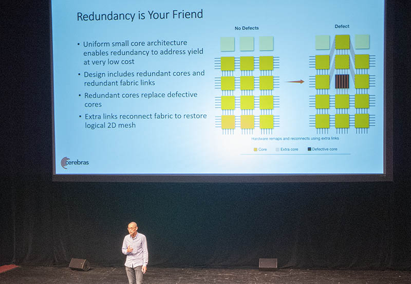
Yield
While AMD and Intel are moving to multi-chip packaging (or what Intel calls glued together chips), to make bigger silicon complexes while maintaining yield. Cerebras is going the other way with a giant chip. As a result, defects are expected on every wafer and therefore every chip. The Cerebras Wafer Scale Engine design expects these defects and has extra cores and interconnect wires to handle these defects.
Using this approach, Cerebras can be “defect tolerant.” While NVIDIA is focused on getting smaller perfect or near-perfect dies, Cerebras designed the Wafer Scale Engine to have multiple defects.
Mas tem outras coisas curiosas
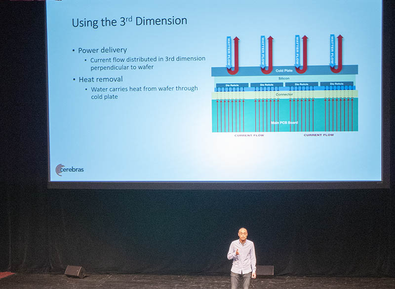
Since the Cerebras Wafer Scale Engine is so big, it cannot be cooled via air and power cannot be delivered using a traditional planar delivery method.
https://www.servethehome.com/cerebras-wafer-scale-engine-ai-chip-is-largest-ever/
Em relação ao sistema propriamente dito mostraram em Dezembro passado ns SC'19
https://www.servethehome.com/cerebras-cs-1-wafer-scale-ai-system-at-sc19/
Só para se ter a noção
Só mesmo naquela da curiosidade, o CEO da Cerebras é o Andrew Feldman.
Would you mind giving our readers a bit of background about yourself and your journey to Cerebras?
Andrew Feldman (AF): Sure. This is my fifth startup. For the last 13 years have been building companies with Gary Lauterbach, who’s our CTO, and one of our founders here.
Before this, I founded a company with Gary, around some of Gary’s ideas, called SeaMicro. We built that over a four year period and we sold that to AMD in 2012. We stayed with AMD for a little while and then took some time off and when we were ready to create again we got some of the band back together again. All the founders were with us at SeaMicro.
https://www.servethehome.com/our-interview-with-andrew-feldman-ceo-of-cerebras-systems/2/
Celebrating One Billion 7nm Chips: Why Scale Matters
https://www.tsmc.com/english/newsEvents/blog_article_20200801.htmTSMC marked an amazing milestone in the past month of July – we manufactured our one-billionth good die on our 7-nanometer (7nm) technology; in layman’s terms, that would be one billion functional, defect-free 7nm chips.
A remarkable achievement for a technology that entered volume production in April 2018. Since then, we have manufactured 7nm chips for well over 100 products from dozens of customers.
Sal para a mesa 7 fáxabor
https://twitter.com/chiakokhua/status/1308216251177512960
a tradução é do tuitteiro acima, o artigo original é de um jornal de Taiwan
https://ctee.com.tw/news/tech/338754.html
https://twitter.com/chiakokhua/status/1308216251177512960
a tradução é do tuitteiro acima, o artigo original é de um jornal de Taiwan
https://ctee.com.tw/news/tech/338754.html
TSMC Reports Third Quarter EPS of NT$5.30
https://www.tsmc.com/tsmcdotcom/PRListingNewsAction.do?action=detail&language=E&newsid=PGWQISPGTHIn US dollars, third quarter revenue was $12.14 billion, which increased 29.2% year-over-year and increased 16.9% from the previous quarter.
Gross margin for the quarter was 53.4%, operating margin was 42.1%, and net profit margin was 38.5%.
...
7-nanometer and 16-nanometer accounted for 35% and 18% respectively. Advanced technologies, defined as 16-nanometer and more advanced technologies, accounted for 61% of total wafer revenue.
Retirado de uma análise Samsung vs TSMC
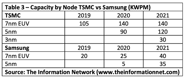
Sub-7nm Node Capacity
Customers
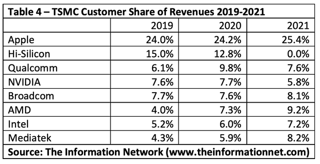
Infelizmente a tabela 4 vem em "Revenue" e não "Capacity", mas bate certo com os rumores de que a capacidade da HiSilicon teria sido dividida entre a AMD e Mediatek.
Sub-7nm Node Capacity
Table 3 shows capacity node for 7nm and lower nodes for TSMC and Samsung. Capacity for TSMC was about 5-6 times greater at the 7nm node in 2019 and 2020 and 3.5 times greater forecasted for 2021. At the 5nm node, TSMC’s capacity is about four times greater.
Customers
TSMC, which serves more than 460 customers, counts its leading customers among the top global fabless companies, including Apple (AAPL), Broadcom (AVG), HiSilicon, AMD (AMD), MediaTek (OTCPK:MDTKF), NVIDIA (NVDA), Qualcomm (QCOM), and Intel (INTC).
Table 4 shows these companies and their percentage of TSMC’s revenues for 2019-2021.
https://seekingalpha.com/article/44...rtake-taiwan-semi-despite-massive-capex-spendIn 2020, Samsung used 60% of its foundry output for internal use, primarily the Exynos chip for its smartphones. The remainder of capacity came from non-captive customers, Qualcomm (20%) and the remaining 20% split among Nvidia, IBM (IBM), and Intel. As Samsung increases its sub 7nm output in 2021, captive consumption will decrease, possibly to 50%.
Infelizmente a tabela 4 vem em "Revenue" e não "Capacity", mas bate certo com os rumores de que a capacidade da HiSilicon teria sido dividida entre a AMD e Mediatek.
Take 2....
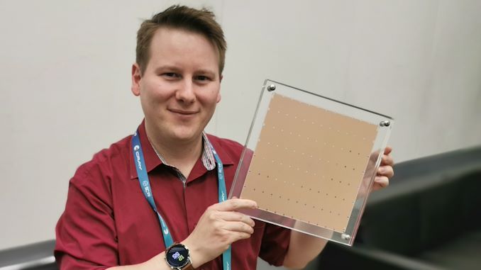
só não dá para aumentar a área.... pois já ocupa toda a wafer (300mm) em pormenor
para comparação


só não dá para aumentar a área.... pois já ocupa toda a wafer (300mm)
em pormenor
para comparação
Miguel_Pereira
Power Member
Isto é basicamente usado como proof of concept, certo? Não é propriamente utilizado ou é?
@Torak post #50
@Miguel_Pereira
@Miguel_Pereira
Neocortex Supercomputer to Put Cerebras CS-1 to the Test
https://www.nextplatform.com/2021/03/30/neocortex-supercomputer-to-put-cerebras-cs-1-to-the-test/Over the next year, we should get a good sense of how the Cerebras CS-1 system performs for dual HPC and AI workloads between installations at Argonne and Lawrence Livermore labs, EPCC, and the Pittsburgh Supercomputing Center (PSC).
Nemesis11
Power Member
O yeld é de 100%, segundo eles. Aliás, parece que a 1ª versão tinha redundância a mais.Isso deve ter um yield de 1 chip per waffer, a correr bem.
Isto não é um "concept". Isto é usado na prática. Eles têm vários deployments feitos e anunciados.Isto é basicamente usado como proof of concept, certo? Não é propriamente utilizado ou é?

Em alguns problemas, parece que é excelente, visto que se consegue correr o problema no mesmo chip e não em centenas ou milhares de nós.
De notar que isto não é um "computador". É mais um acelerador externo. Uma comparação simples. É +/- como ter uma Gráfica externa ligada por Thunderbolt a um computador.
Ele precisa de estar ligado a 7 a 8 Servidores + Storage Externa muito rápida, ligado com 12 Links 100 Gbits.
O preço deste "acelerador externo" ronda os 2.5 milhões de $, fora o resto à volta (Servidores, Storage, etc).
Não está aí, mas consome 23 KW e tem "canalização" interna completamente redundante.
O Ian tem um video sobre ele:
Os 6nm da TSMC já estão a bombar
MediaTek Launches 6nm Dimensity 1200 Flagship 5G SoC with Unrivaled AI and Multimedia for Powerful 5G Experiences
Premium Performance: The Dimensity 1200 has an octa-core CPU designed with an ultra-core Arm Cortex-A78 clocked up to 3GHz for extreme performance, three Arm Cortex-A78 super cores and four Arm Cortex-A55 efficiency cores. With a nine-core GPU and six-core MediaTek APU 3.0, the Dimensity 1200 delivers a new level of premium performance. The Dimensity 1100 is designed with an octa-core CPU which includes four Arm Cortex-A78 cores operating at up to 2.6GHz and four Arm Cortex-A55 efficiency cores, along with a nine-core Arm Mali-G77 GPU. Both chipsets are manufactured on TSMC’s advanced 6nm process technology.