
dead_mouse
Power Member
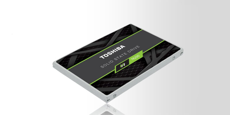
Com um quadradito de fita térmica só para o controlador... parece mesmo budget oriented...
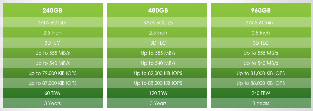
Se comparares com ssd's da mesma capacidade, estes mlc têm mais endurance.
 : http://www.guru3d.com/news-story/1-petabyte-write-enhanced-nvme-m-2-ssd-released-by-atp.html
HoT se queres endurance tens isto
http://www.digitimes.com/news/a20171016PD205.htmlToshiba recently suspended NAND flash production at its Japan facilities for a few weeks due to ransomware attacks on its computer network, according to sources at channel distributors. The incident could tighten global NAND flash supply.
Toshiba decided to shut down the production for 3-6 weeks to deal with the hacking, but production has now returned to normal, said the sources, adding that the suspension resulted in reduced NAND flash production nearly 100,000 wafers.
http://www.digitimes.com/news/a20171016VL202.htmlToshiba announced recently its board of directors had approved a further investment by Toshiba Memory in production equipment for Fab 6 at its Yokkaichi operations in Mie (Japan).
Toshiba's Fab 6, which is still under construction, will be dedicated to producing the company's 3D flash memory.
Toshiba Memory will invest about JPY110 billion (US$984.4 million) as a second investment in Fab 6 for the installation of additional manufacturing equipment in the phase-1 cleanroom, Toshiba said.
Yangtze River Storage Technology (YMTC) under the Tsinghua Unigroup has successfully developed 32-layer 3D NAND flash chips, marking a new milestone and major technological breakthrough in China's memory-chip industry, according to industry sources.
http://www.digitimes.com/news/a20171115PD207.htmlThe company has completed equipment installation and is slated to kick off trial production in the second quarter of 2018, with initial capacity set at 5,000 pieces per month. It will start mass production after achieving stable yield rates, the sources said.

The company’s $26 billion in 2017 outlays expected to be more than Intel and TSMC combined.
...
After spending $11.3 billion in semiconductor capex last year, Samsung announced that its 2017 outlays for the semiconductor group are expected to more than double to $26 billion.
http://www.icinsights.com/news/bull...i-Capex-Deliver-Knockout-Blow-To-Competition/IC Insights estimates that Samsung’s $26 billion in semiconductor outlays this year will be segmented as follows:
3D NAND flash: $14 billion (including an enormous ramp in capacity at its Pyeongtaek fab)
DRAM: $7 billion (for process migration and additional capacity to make up for capacity loss due to migration)
Foundry/Other: $5 billion (for ramping up 10nm process capacity)

")